
AMD Taps GlobalFoundries for MI500 Co Packaged Optics as Silicon Photonics Competition With NVIDIA Intensifies
AMD is reportedly preparing a major optical interconnect shift for its future Instinct MI500 accelerators, with new supply chain reporting indicating that the company will work with GlobalFoundries on a co packaged optics solution built around photonic integrated circuits, while ASE is expected to handle packaging. At this stage, the GlobalFoundries and ASE involvement appears to come from industry reporting rather than a formal AMD product announcement, so it should be treated as a report, not a fully confirmed deployment plan. What is confirmed is that AMD has been actively investing in co packaged optics, including its earlier acquisition of Enosemi, which AMD said would help it scale photonics and co packaged optics development across next generation AI systems.
That distinction matters because co packaged optics is quickly becoming one of the most important battlegrounds in AI infrastructure. Traditional copper interconnects are increasingly running into power, latency, and bandwidth limits as accelerator clusters grow larger and denser. Co packaged optics aims to solve that by moving optical communication much closer to the compute package itself, reducing electrical losses and enabling faster, more power efficient data movement across AI systems. GlobalFoundries has been publicly expanding its silicon photonics positioning through its GF Fotonix platform and related advanced packaging initiatives, which makes the reported AMD connection strategically plausible even if the MI500 specific manufacturing arrangement has not yet been publicly confirmed by AMD itself.
For AMD, the broader roadmap behind this report is already on the record. At CES 2026, AMD said its Instinct MI500 series is planned for 2027 and is on track to deliver up to 1000x AI performance compared with the MI300X introduced in 2023. The company also stated that MI500 will use CDNA 6, advanced 2nm process technology, and HBM4E memory. Those details are official, and they show that AMD is treating MI500 as far more than a routine generation update. It is being framed as a foundational product for the next phase of large scale AI infrastructure.
This is where the co packaged optics angle becomes especially important. If AMD is indeed pairing MI500 with an MRM based optical design, that would suggest the company is targeting not just raw compute leadership, but also the interconnect efficiency needed for much larger AI fabrics. In other words, the real competition is no longer only about how fast a single GPU can run. It is about how effectively thousands of accelerators can communicate across a rack, a pod, and eventually a full AI factory. That is the same strategic direction being discussed around NVIDIA’s Vera Rubin generation, where the surrounding memory and optical ecosystem is becoming just as important as the accelerator itself. Public reporting has also suggested NVIDIA is pursuing similar optical integration paths, although exact implementation details vary by report and not all have been formally confirmed.
AMD’s acquisition of Enosemi last year now looks even more relevant in that context. The company explicitly said the deal would accelerate co packaged optics innovation for AI systems, and Reuters similarly reported that the move was part of AMD’s strategy to strengthen its optics capabilities for AI infrastructure. That means even if the specific GlobalFoundries, ASE, and MI500 supply chain details remain in the reporting phase, the larger direction of travel is already established. AMD is clearly building toward optical interconnect integration as AI systems scale beyond what copper can handle efficiently.
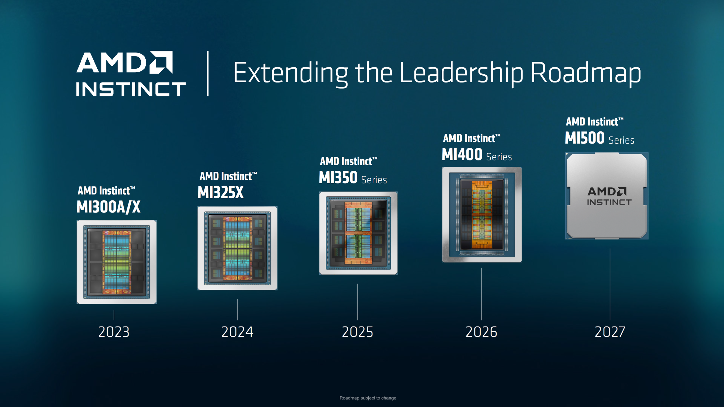
The competitive pressure is obvious. NVIDIA continues to push aggressively on rack scale AI systems, and AMD is responding by expanding its platform story around compute, memory, and now potentially optics. If MI500 launches in 2027 with CDNA 6, HBM4E, advanced 2nm production, and a meaningful optical interconnect strategy, it could become one of AMD’s most important AI products yet. The challenge, as always, will be execution. Co packaged optics is one of the most promising technologies in the industry, but it is also one of the most complex to manufacture and scale. That is why the reported involvement of GlobalFoundries and ASE stands out. It would give AMD access to partners with clear momentum in silicon photonics and advanced packaging at a time when optical interconnects are becoming a strategic necessity rather than a future experiment.
For now, the safest reading is this: AMD has officially confirmed the MI500 timeframe, architecture class, process node, and memory direction, while the reported use of GlobalFoundries for photonic integrated circuits and ASE for packaging should still be treated as supply chain reporting until AMD says more publicly. Even so, the signal is strong. The AI race is moving beyond silicon alone, and the companies that win the next round may be the ones that solve interconnect bottlenecks just as effectively as they solve compute performance.
Do you think co packaged optics will become a standard feature for top tier AI accelerators by 2027, or will adoption still be limited to the most advanced data center deployments?