
Sub 1nm Logic Roadmap Points to 2034 Debut, With 2D FET Era Targeted for 2043 to 2046
The semiconductor industry is not about to break into sub 1nm manufacturing overnight, but the next stage of logic scaling is clearly taking shape. A new roadmap tied to IMEC shows that the first 0.7nm class logic node is now projected for around 2034, with 0.5nm following around 2036, 0.3nm around 2040, and 0.2nm class technology entering the picture in the 2043 to 2046 window. IMEC, founded in 1984, describes itself as the world’s largest independent research and innovation center for nanoelectronics and digital technology, which makes its long range logic outlook one of the more influential signals for where advanced silicon is heading next.
What stands out in this roadmap is not just the timeline, but the message behind it: Moore’s Law is still alive, yet it is no longer being driven by the easy, fast horizontal scaling gains the industry enjoyed in earlier decades. Instead, future progress will come from a mix of transistor architecture changes, new interconnect materials, backside power delivery strategies, and deeper system level integration. In practical terms, this means the race is no longer only about shrinking dimensions. It is about finding viable ways to sustain density, power efficiency, and performance when the physical and economic limits of conventional scaling are becoming harder to overcome.
In the near term, the industry remains focused on gate all around nanosheet transistors. IMEC notes that the nanosheet family can continue the logic scaling roadmap for at least 3 technology generations when combined with innovations at standard cell level. That places nanosheets as the bridge between the last FinFET era and the first true sub 1nm class nodes. In other words, the current angstrom transition is still very much a nanosheet story before the next architectural pivot arrives.
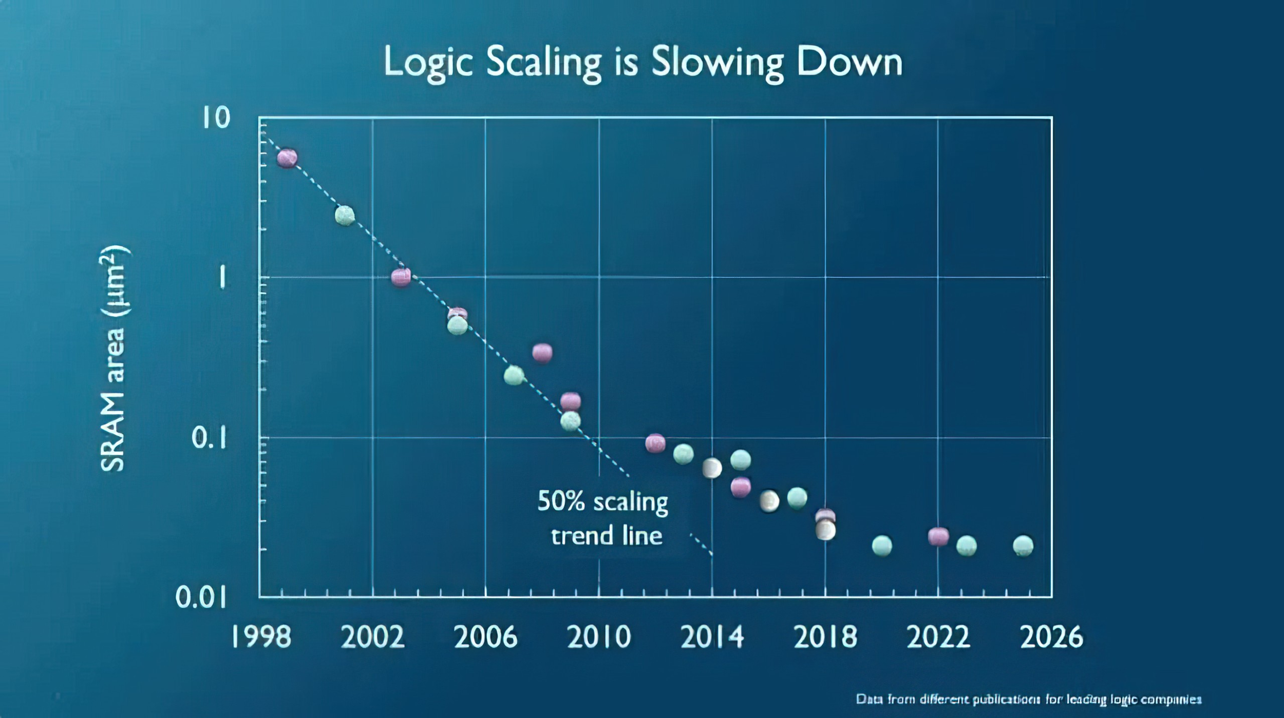
That next pivot is CFET, or complementary FET. According to IMEC, CFET architectures are expected to succeed gate all around nanosheet transistors, with nMOS and pMOS devices stacked vertically. This is a major change because it removes n and p separation from standard cell height considerations and opens the door to substantially smaller logic cell sizes. IMEC’s more recent work specifically studies monolithic CFET scaling for A7, A5, and A3 logic nodes, reinforcing the idea that the first sub 1nm generation will not simply be a refined nanosheet node, but a structural shift in how logic transistors are built.
For readers tracking the commercial side of the market, the key takeaway is that sub 1nm is still a long game. The roadmap points to around 2034 for A7 or 0.7nm class logic, which is well beyond the current 2nm and angstrom class transitions now being prepared by leading foundries. This also helps explain why advanced packaging, chiplets, thermal management, and memory proximity are becoming so central to AI and HPC platform design today. Logic scaling is continuing, but it is no longer the only lever that matters.
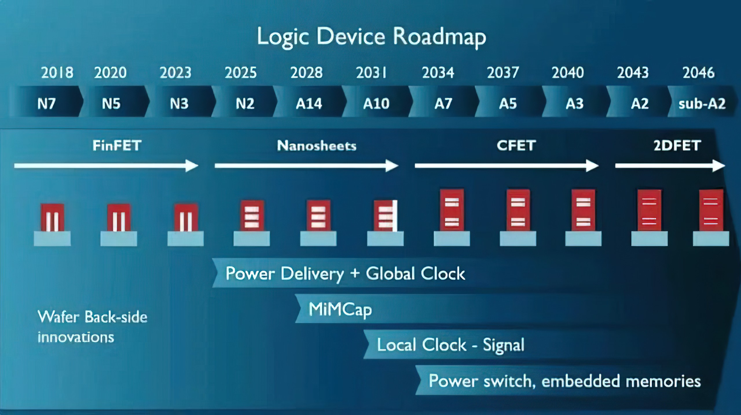
The roadmap becomes even more ambitious after CFET. IMEC says 2D material based devices are a promising option to extend the logic roadmap further, and its current strategy looks toward introducing 2D materials in stages before eventually using them in advanced architectures. In its published research, IMEC discusses introducing planar 2D devices earlier, while also preparing for the long term shift toward 2D channel materials in more advanced nodes. That is why the 2043 to 2046 window matters so much: it represents the point where the industry may move from refined silicon channel engineering into a more radical materials transition.
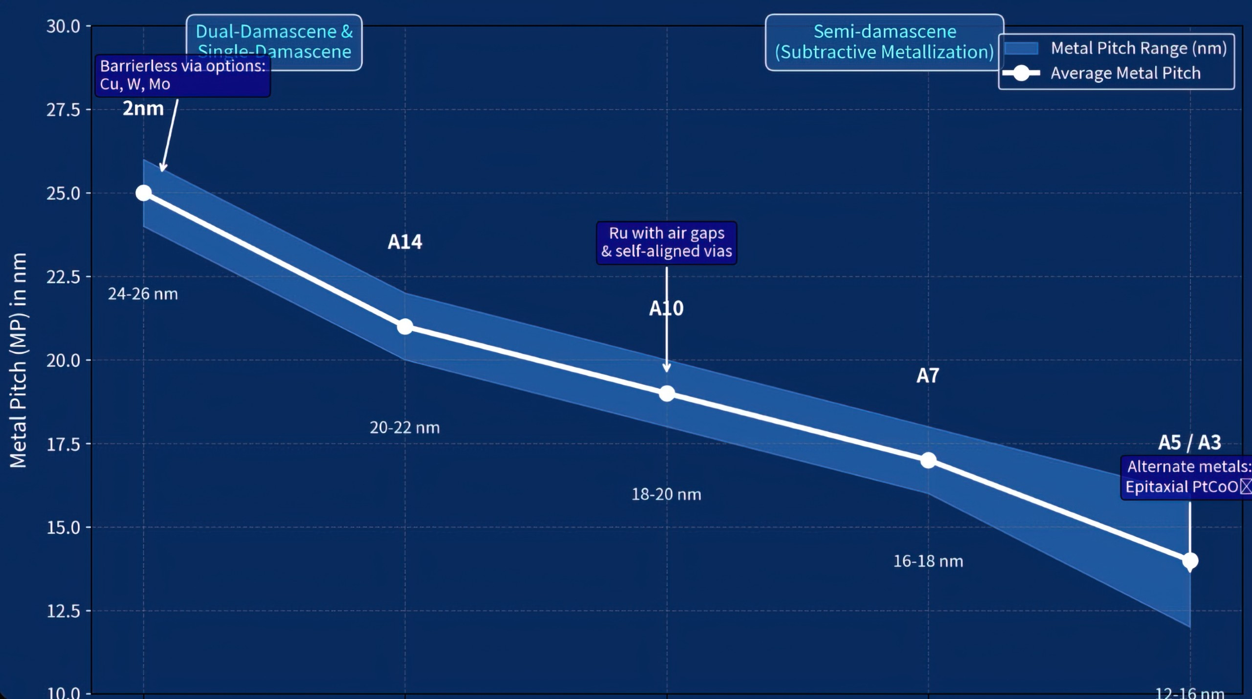
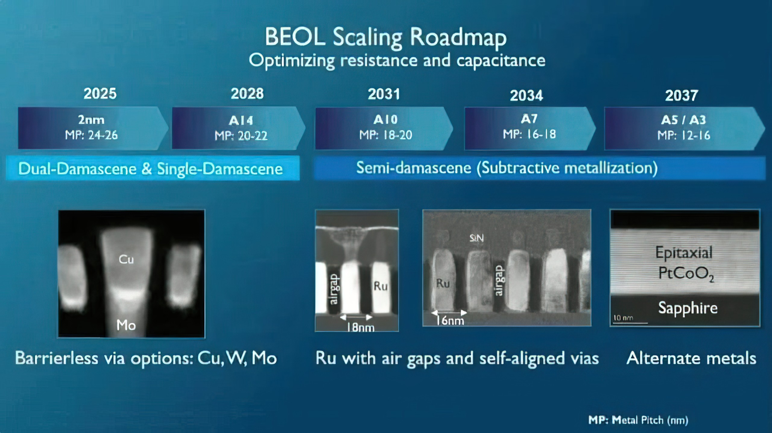
Interconnect technology is evolving just as aggressively. IMEC has long argued that advanced logic architectures will immediately affect local interconnect layers and require novel BEOL materials such as ruthenium, molybdenum, and metal alloys, along with integration approaches such as semi damascene. In 2025, IMEC demonstrated 16nm pitch ruthenium lines using a semi damascene flow, describing this as a promising approach for A7 and beyond logic nodes. That matters because at these scales, wiring resistance and capacitance become just as critical as transistor innovation. A better transistor is not enough if the metal stack becomes the bottleneck.
This is where the roadmap becomes particularly relevant for AI hardware. The future of compute is not just about packing more transistors into a smaller area. It is also about getting power into the chip more efficiently, moving data across the package with less loss, and keeping thermals under control while performance keeps climbing. That broader systems view is exactly why advanced logic, BEOL innovation, and packaging are increasingly being discussed together rather than as separate technology tracks.
Below is a simplified view of the logic roadmap described in the report:
| Year | Node | Architecture | Main Transition |
|---|---|---|---|
| 2025 | 2nm | Nanosheet FET | Gate all around era begins |
| 2028 | A14, 1.4nm | Improved nanosheet FET | Further density scaling |
| 2031 | A10, 1.0nm | Advanced nanosheet FET | Last major nanosheet class step |
| 2034 | A7, 0.7nm | CFET | First sub 1nm class transition |
| 2036 to 2037 | A5, 0.5nm | CFET | Continued vertical transistor stacking |
| 2040 | A3, 0.3nm | CFET | Further density and integration gains |
| 2043 | A2, 0.2nm | 2D FET | First major 2D material node target |
| 2046 | Below A2, under 0.2nm | Advanced 2D FET | Beyond 0.2nm scaling target |
This is the simplified BEOL direction highlighted alongside the transistor roadmap:
| Year | Node | Metal Pitch | Interconnect Direction |
|---|---|---|---|
| 2025 | 2nm | 24 to 26nm | Dual and single damascene, copper based |
| 2028 | A14 | 20 to 22nm | Continued conventional scaling |
| 2031 | A10 | 18 to 20nm | Transition toward semi damascene |
| 2034 | A7 | 16 to 18nm | Ruthenium, self aligned vias, air gap integration |
| 2037 and beyond | A5 to A3 | 12 to 16nm | Alternate metals and more advanced interconnect schemes |
The bigger picture is clear: sub 1nm logic is coming, but not soon enough to carry the full burden of performance growth on its own. Between now and 2034, the real battle will be fought across transistor structure, interconnect materials, advanced packaging, power delivery, and memory integration. For gamers, creators, and AI infrastructure watchers, that means future leaps in performance will likely come from platform level engineering as much as from the process node stamped on the box.
What do you think will matter more in the next 10 years, smaller process nodes or smarter chip architecture and packaging?