
Intel Shows Dual Crescent Island GPUs on Liquid Cooled OAM Module With First Xe3P Die Photos
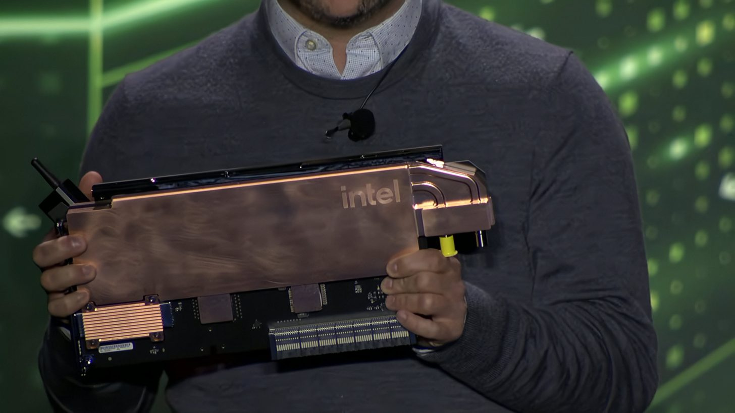
Intel has showcased a new dual GPU Crescent Island accelerator at the 2026 Open Compute Project Global Summit, combining 2 Xe3P GPUs on a single liquid cooled OAM module. The demonstration introduces another configuration for Intel's recently announced GPU D Series, alongside the first physical die photographs of its next generation AI architecture. The design targets high density AI inference infrastructure rather than conventional gaming or workstation graphics.
The OAM (OCP Accelerator Module) features 2 Crescent Island GPUs, each surrounded by dedicated LPDDR5X memory, with onboard bridging hardware and a mezzanine connector. A large copper cooling assembly covers both processors, providing liquid cooling for the compact dual GPU configuration. Unlike Intel's standard air cooled PCIe reference card, this design demonstrates how manufacturers could integrate multiple Xe3P accelerators into more specialized AI servers. However, Intel has not disclosed the OAM module's combined power consumption, memory capacity, interconnect bandwidth, or commercial availability.
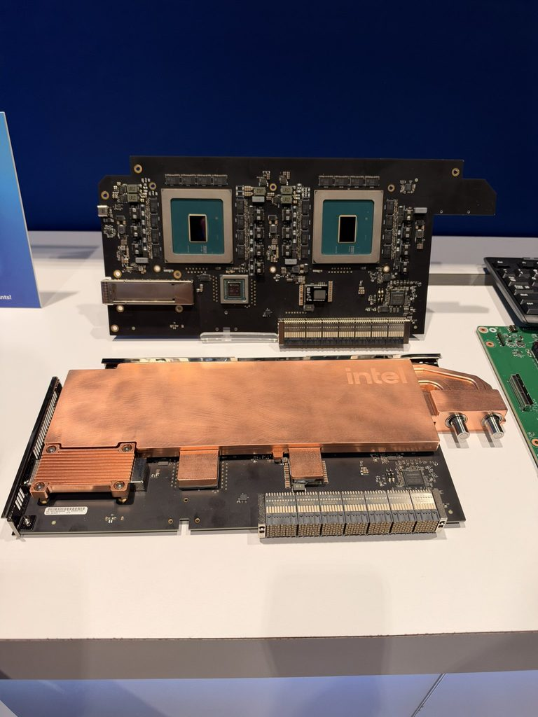
Intel Crescent Island PCIe vs Dual GPU OAM
| Specification | PCIe D270 Reference | Dual GPU OAM |
|---|---|---|
| GPU Architecture | Xe3P | Xe3P |
| GPU Count | 1 | 2 |
| Form Factor | PCIe 5.0 card | OAM module |
| Cooling | Air cooling | Liquid cooling |
| Memory | 160 GB LPDDR5X reference | Dedicated LPDDR5X per GPU |
| Power | 350 W | Not disclosed |
| Status | Customer sampling underway | Demonstration design |
Intel specifies up to 480 GB LPDDR5X per GPU for supported configurations. The memory capacity and performance of the dual GPU OAM module have not been confirmed.
According to Intel's official OCP announcement, Crescent Island, now branded as the Intel GPU D Series, delivers up to 1.3 PFLOPS of FP8 compute, 1.5 TB/s memory bandwidth, and 480 GB LPDDR5X capacity per GPU. Its Xe3P architecture features 32 Xe cores and 256 XMX matrix engines, prioritizing AI inference, large language models, and memory intensive workloads, capabilities were detailed in the Intel GPU D270 specifications.
The newly revealed die photographs also provide a closer look at the Xe3P processor, reportedly manufactured using TSMC's N3P process. Initial visual comparisons suggest the chip may be smaller than Intel's Battlemage BMG G31 GPU, although official die dimensions have not been published. As explained in the Xe3P architectural analysis by Chips and Cheese, Intel has expanded its matrix acceleration hardware while optimizing the architecture for AI computing rather than traditional graphics workloads.
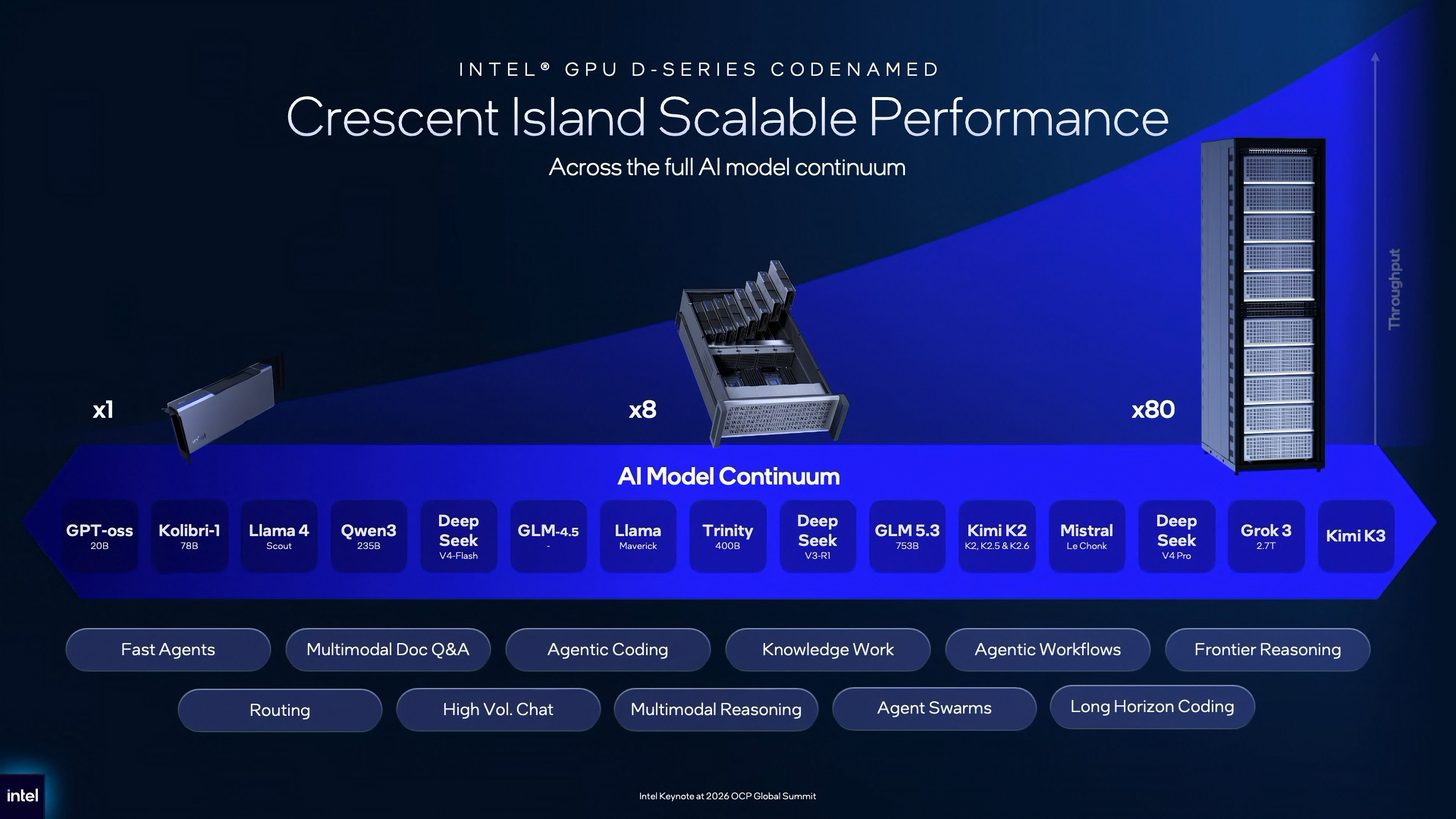
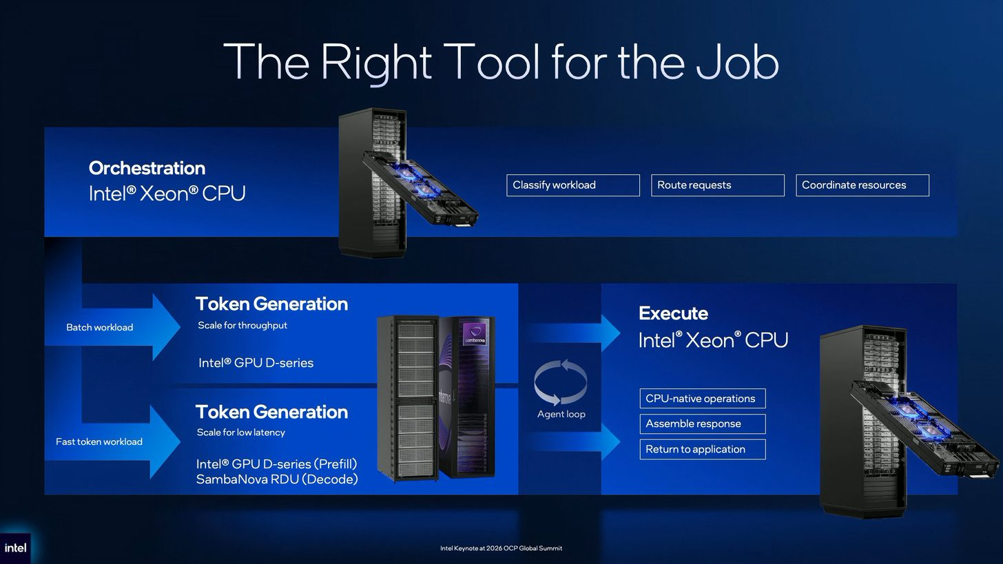
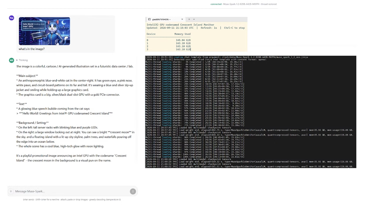
Intel is also expanding its software ecosystem through open AI frameworks and partnerships supporting larger accelerator deployments. Customer sampling is underway, but the company has not confirmed pricing or general commercial availability for the dual GPU OAM design.
The dual GPU OAM demonstration suggests Intel is looking beyond conventional PCIe accelerators toward higher density AI infrastructure. Combining multiple Xe3P processors with LPDDR5X memory and liquid cooling could give server manufacturers more flexibility when building systems for large AI models and concurrent inference workloads.
The interesting distinction is Intel's continued reliance on LPDDR5X rather than HBM. This prioritizes memory capacity and potentially lower system costs, although bandwidth remains considerably below flagship HBM equipped accelerators.
However, the dual GPU design still needs validated performance figures, power specifications, and software scaling results. Its commercial potential will depend on how effectively Intel can translate the hardware into competitive inference performance and operating costs.
Could Intel's high capacity LPDDR5X accelerators become a competitive alternative to NVIDIA and AMD's HBM based AI GPUs, or will memory bandwidth remain the deciding factor?
