
Intel Processes 1 Million High NA EUV Wafers as Early Adoption Pulls Ahead of TSMC and Samsung
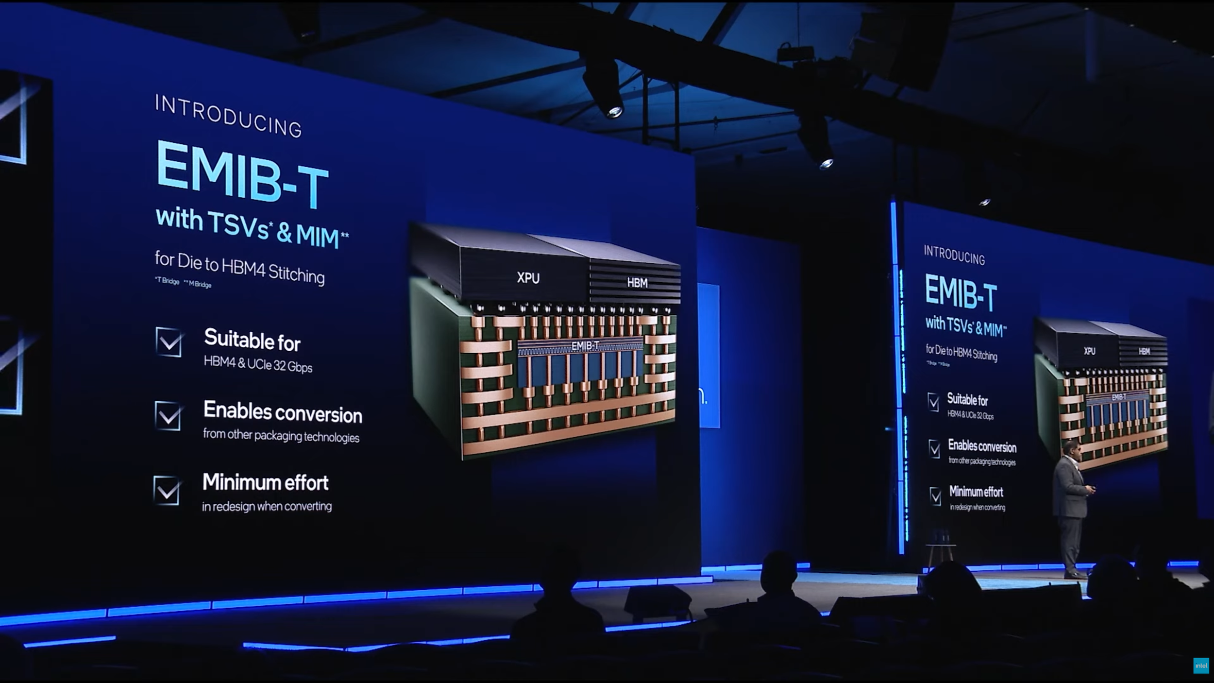
Intel Foundry has passed a major semiconductor manufacturing milestone, processing more than 1 million 300 mm wafers using ASML High NA EUV lithography as its early investment in the technology begins moving from research into commercial production. The figure covers wafers processed during initial equipment certification, research and development, and volume manufacturing, including selected layers of Intel Core Ultra Series 3 Panther Lake processors. Intel is currently the first logic manufacturer shipping high volume products incorporating High NA EUV, giving the company considerably more practical manufacturing experience with the technology than TSMC and Samsung currently possess.
Intel and ASML announced the milestone during the SPIE Photomask Technology and Extreme Ultraviolet Lithography conference. Intel says overlay accuracy, throughput, and equipment availability are currently meeting its expectations, while Intel 18A layers produced with High NA are achieving performance that meets or exceeds equivalent layers patterned using conventional 0.33 numerical aperture EUV equipment. That is particularly significant because Intel is no longer evaluating the technology exclusively through experimental wafers. High NA is now operating inside a real manufacturing flow.
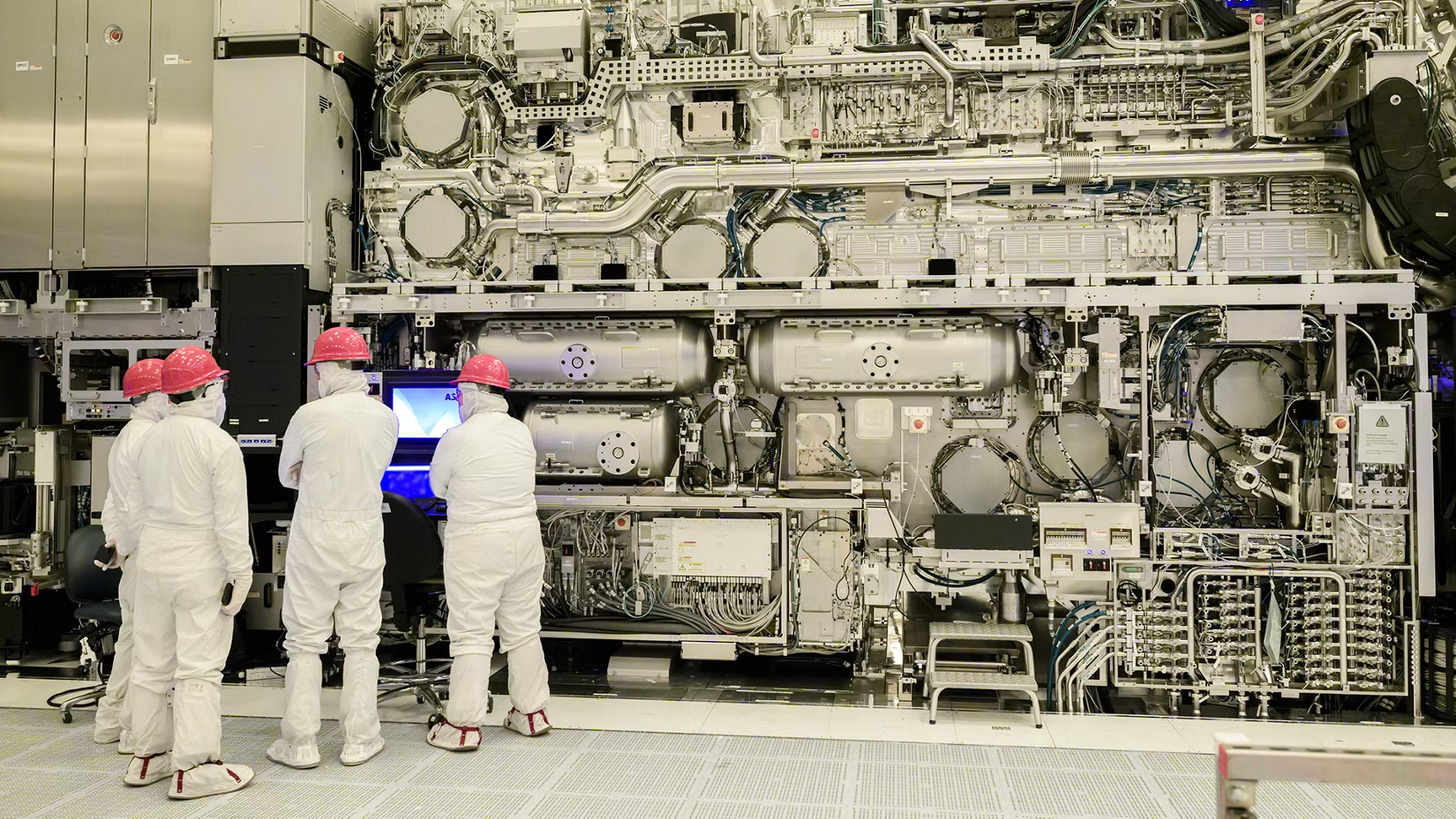
Intel installed the industry's first commercial ASML High NA EUV system at its Oregon research facility in 2024 and later became the first semiconductor manufacturer to install and complete acceptance testing of the second generation TWINSCAN EXE:5200B. In July 2026, ASML confirmed that High NA EUV had entered volume manufacturing with Intel Panther Lake, with selected Intel 18A layers qualified on both High NA EXE equipment and conventional NXE EUV systems. Products using those layers are already shipping to customers.
"The first high volume logic product manufactured with High NA."
— Quote by: Christophe Fouquet, ASML President and CEO
#Samsung plans to move to $ASML advanced High NA EUV machine in 2028 and $TSM in 2030.
— Mojo (@Mojo_flyin) September 8, 2026
Meanwhile @Intel_Foundry today announced they have outputted 1 mln wafers across research, test and volume production on High NA.@Intel has at least a 2-4 year advantage here.$INTC pic.twitter.com/gXbLLM2yn5
High NA increases numerical aperture from 0.33 to 0.55, allowing ASML's EXE platform to resolve considerably smaller features. The technology can produce structures approximately 1.7 times smaller while potentially enabling around 2.9 times greater transistor density compared with conventional EUV. More importantly for manufacturing, patterns that might otherwise require multiple exposures can potentially be produced using fewer lithography steps, reducing process complexity as semiconductor nodes continue scaling.
Intel's position contrasts sharply with the more cautious adoption strategies at TSMC and Samsung. TSMC continues to extend conventional EUV for its upcoming A14 generation and is not expected to introduce High NA into meaningful manufacturing until later in its roadmap. Samsung has also delayed broad foundry deployment, with the company previously indicating that conventional EUV should remain its primary approach through much of its 1.4 nm development before High NA becomes increasingly necessary around future 1 nm class technologies. Memory manufacturers are moving somewhat faster, with Samsung and SK hynix evaluating High NA for advanced DRAM production ahead of broader logic adoption.
This creates the basis for estimates placing Intel approximately 2 to 4 years ahead in practical High NA manufacturing experience, but that comparison requires context. Intel has unquestionably entered production earlier, while TSMC and Samsung have deliberately chosen to delay broader deployment because conventional EUV remains economically competitive for their current process roadmaps. A timing advantage therefore does not automatically translate into a process technology lead or guarantee that Intel will produce better chips than its competitors.
Intel is also working with ASML on one of High NA's largest remaining manufacturing challenges. The 0.55 numerical aperture optical system reduces the exposure field compared with current EUV equipment, which can require large chip designs to be divided and joined through stitching. Intel currently supports High NA using conventional 6 inch masks with either careful die placement or stitching, but the company has spent more than 3 years pushing the semiconductor ecosystem toward larger 6 × 12 inch masks. These larger masks could eventually restore full field exposure for large processors and simplify High NA manufacturing for increasingly massive AI and data center silicon.
The milestone also strengthens Intel Foundry's argument that its early High NA investment has practical value beyond internal processor manufacturing. External customers considering future Intel process technologies would gain access to a lithography infrastructure that has already accumulated substantial manufacturing data before competing foundries begin their own major production ramps. The challenge for Intel remains converting that technical experience into competitive yields, manufacturing costs, capacity, and meaningful external foundry volume.
The broader High NA race is also expanding beyond logic processors. SK hynix recently installed an ASML TWINSCAN EXE:5200B at its M16 facility as part of its next generation DRAM development, a milestone we covered when SK hynix began integrating High NA EUV into its production infrastructure. High bandwidth memory, AI accelerators, and increasingly dense logic designs are likely to become major drivers for the technology as conventional EUV reaches increasingly difficult economic and technical limits.
Processing more than 1 million High NA wafers matters because Intel has moved beyond claiming an equipment advantage and is now building manufacturing experience that competitors cannot obtain simply by purchasing the same ASML scanner later.
TSMC and Samsung may ultimately prove correct that delaying High NA reduces costs while conventional EUV remains competitive. Intel is effectively making the opposite bet. It is accepting the enormous cost and complexity of early adoption in exchange for several years of process development, equipment optimization, stitching experience, mask ecosystem development, and production data.
That experience could become particularly valuable around Intel 14A and future nodes, where High NA is expected to play a considerably larger role. The real victory will not be owning the first machines or processing the most wafers. It will come if Intel can translate that head start into better density, competitive yields, lower manufacturing complexity, and enough confidence to attract major external foundry customers.
Will Intel's early High NA EUV investment become a genuine manufacturing advantage, or are TSMC and Samsung making the smarter move by waiting for the technology to mature?
