
Innosilicon LPDDR6 and LPDDR5X Memory Controller IP Delivered To First Customers, Targeting Up To 14.4 Gbps
Chinese chip maker Innosilicon has announced that its LPDDR6 and LPDDR5X memory controller IP has been delivered to its first domestic customers, marking what the company describes as its first domestic commercial cooperation for this next generation mobile and low power memory interface stack.
Innosilicon first revealed its LPDDR6 and LPDDR5X PHY and controller IP offering in 2025, positioning the combo as a foundation for upcoming platforms that need higher bandwidth without blowing up power budgets. In the new update, the company frames the LPDDR6 and LPDDR5X PHY plus controller combo as a multi packaged controller solution designed around advanced FinFET process technology. The pitch is clear and directly aligned with what modern mobile SoCs and edge AI chips are chasing: low power operation, high bandwidth, and low latency, backed by a longer track record across high speed memory adjacent technologies like GDDR6, GDDR6X, GDDR7, plus HBM3E and HBM4 experience that Innosilicon says helped harden its LPDDR6 and LPDDR5X roadmap for mass market deployment.
From a features perspective, the company highlights a fairly comprehensive LPDDR6 specific capability set aimed at performance scaling and reliability. This includes I O speed support up to 14.4Gbps, ECS support in both auto and manual modes plus Link ECC, system meta function mode, multiple refresh options including dual, per, and all bank refresh in single and burst behaviors, read modify write with mask write, dynamic write NT ODT, DVFSL mode, and burst modes spanning x24 and x48. On the common feature side shared across LPDDR6 and LPDDR5X, Innosilicon calls out flexible data width expansion from x12 to x48 for LPDDR6 and x16 to x32 for LPDDR5X, built in performance monitoring, Tx pre emphasis and Rx DFE signal conditioning for improved integrity, LPDDR5X WCK mode plus Link ECC support, package options covering PoP and discrete memory, single rank and multi rank configurations, PVT compensation and timing calibration across corners, at speed BIST with scan insertion and loopback support, multiple low power modes including idle auto gating plus self refresh and power down retention, and configurable register interfaces via APB, AHB, and AXI.
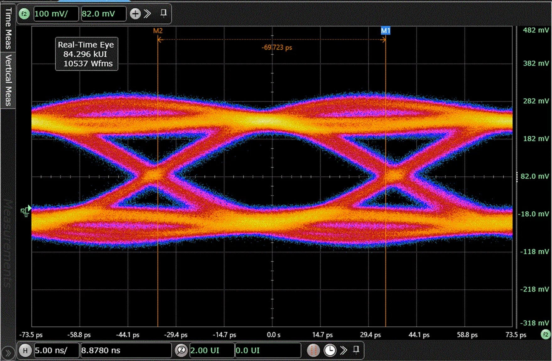
The most headline grabbing claim is the throughput jump to 14.4Gbps, which Innosilicon attributes to a custom I O architecture design combined with process optimizations guided by SIPI simulation. The company says these choices enable a 1.5x increase versus its existing LPDDR5X solution that tops out at 9.6Gbps. It also points to an architectural shift in LPDDR6 from 16 bit to 24 bit, describing how the I O rate scales from 9.6Gbps to 14.4Gbps while the I O bit size expands from 8 bit to 12 bit. Innosilicon’s framing is that this results in a single channel 24 bit architecture delivering a 2x bandwidth bump, which is the kind of upgrade path that should matter for GPU class integrated graphics, on device AI workloads, and content creation heavy mobile pipelines that increasingly behave like handheld gaming PCs in terms of bandwidth appetite.
Commercially, Innosilicon states its LPDDR6 and LPDDR5X IP is on track for mass production readiness, with first products using the technology expected to launch in 2026 from several partners. The company also claims it has developed a new framework that reduces product development cycles by 30%, aiming to help customers compress time to market for new silicon launches.
For gamers and hardware watchers, this is one of those ecosystem moves that matters even if it does not immediately land in a retail product you can buy tomorrow. Memory controller IP is the behind the scenes unlock that determines what SoCs can realistically ship at scale, and 14.4Gbps class LPDDR6 capability is the type of stepping stone that can influence everything from flagship phones to next generation handheld gaming devices and thin laptops that want more bandwidth without moving to higher power memory configurations.
What do you think is the bigger win for LPDDR6 in real world devices, the 14.4Gbps speed target, the 24 bit architecture shift, or the reliability features like Link ECC and calibration across corners?