
TSMC Previews A13 and A12 for 2029 While Extending Current EUV Further Instead of Moving to High NA
TSMC has outlined a broader long term process and packaging roadmap at its 2026 North America Technology Symposium, confirming that A13 and A12 are both planned for 2029 while the company continues extracting more value from its existing EUV strategy rather than jumping to ASML’s most expensive High NA tools right away. The update signals a very deliberate approach from the foundry leader: keep advancing density, power, and packaging at scale, but avoid adopting High NA until the cost and technical return make clearer business sense.
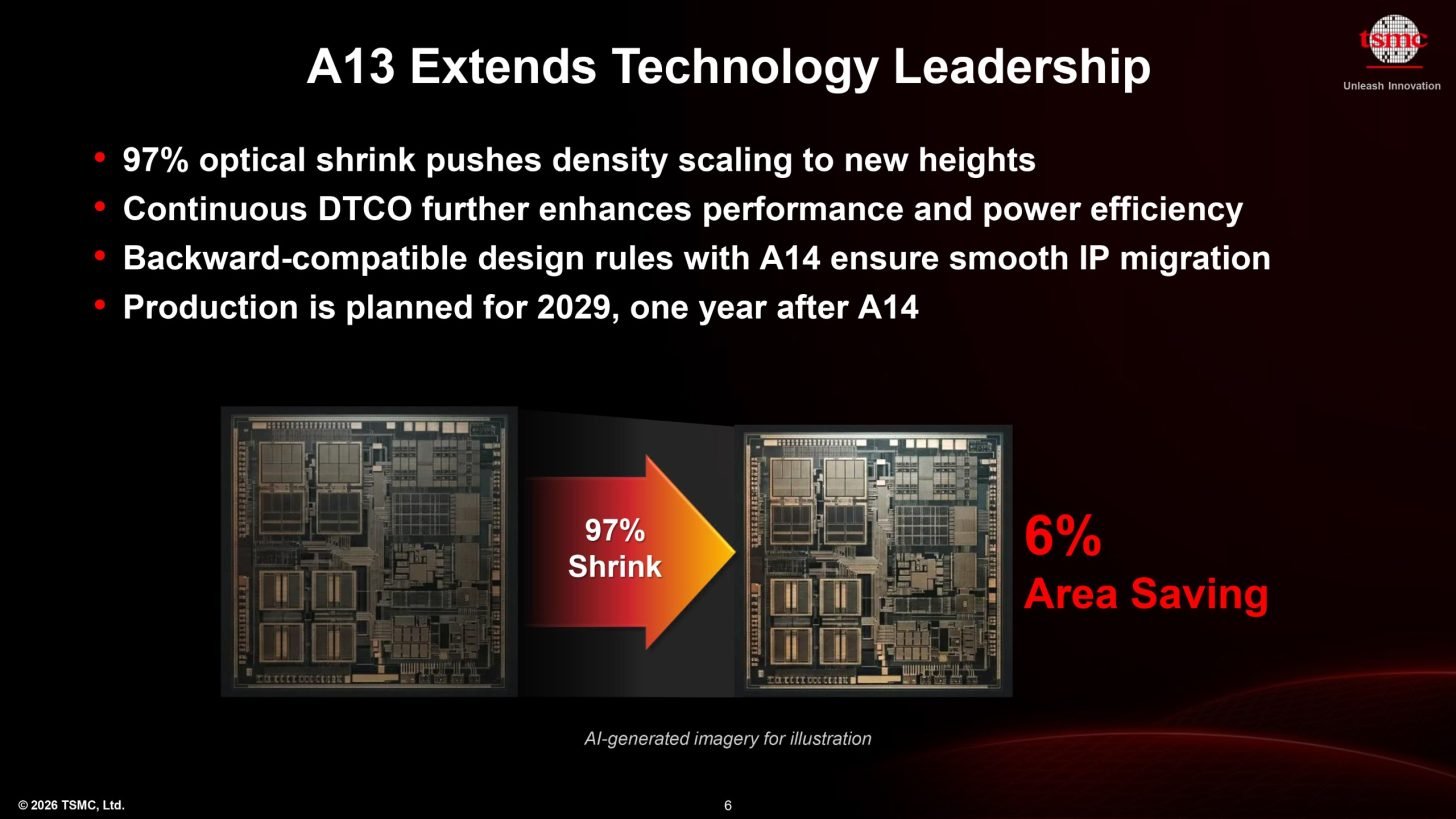
The headline process announcement is A13. TSMC says A13 is a direct shrink of A14 and will provide 6% area savings versus A14, while keeping design rules fully backward compatible so customers can move designs over more quickly. The company is also positioning A13 for next generation artificial intelligence, high performance computing, and mobile products, with production scheduled for 2029, 1 year after A14. That makes A13 less of a radical architectural break and more of a disciplined refinement node aimed at maximizing customer design reuse while still pushing density and efficiency forward.
TSMC also previewed A12 as an enhancement of the A14 platform. The most important detail there is the inclusion of Super Power Rail for backside power delivery, aimed at AI and HPC applications, with production also targeted for 2029. That tells us TSMC is continuing to separate its roadmap into nodes and follow on enhancements that can better serve different workload classes, especially where AI chips need stronger power delivery and tighter scaling without forcing customers into a totally new design jump every year.
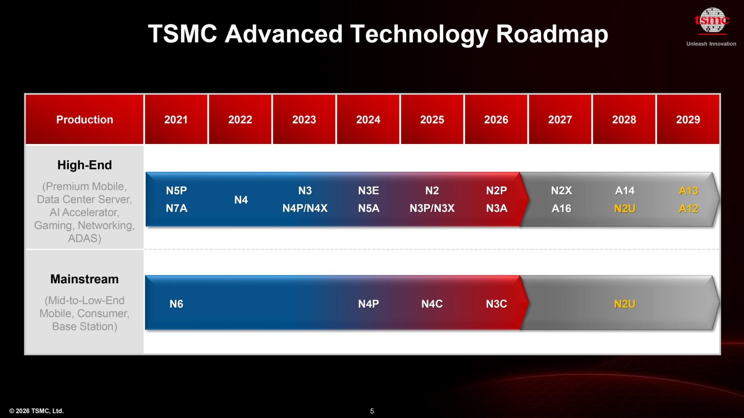
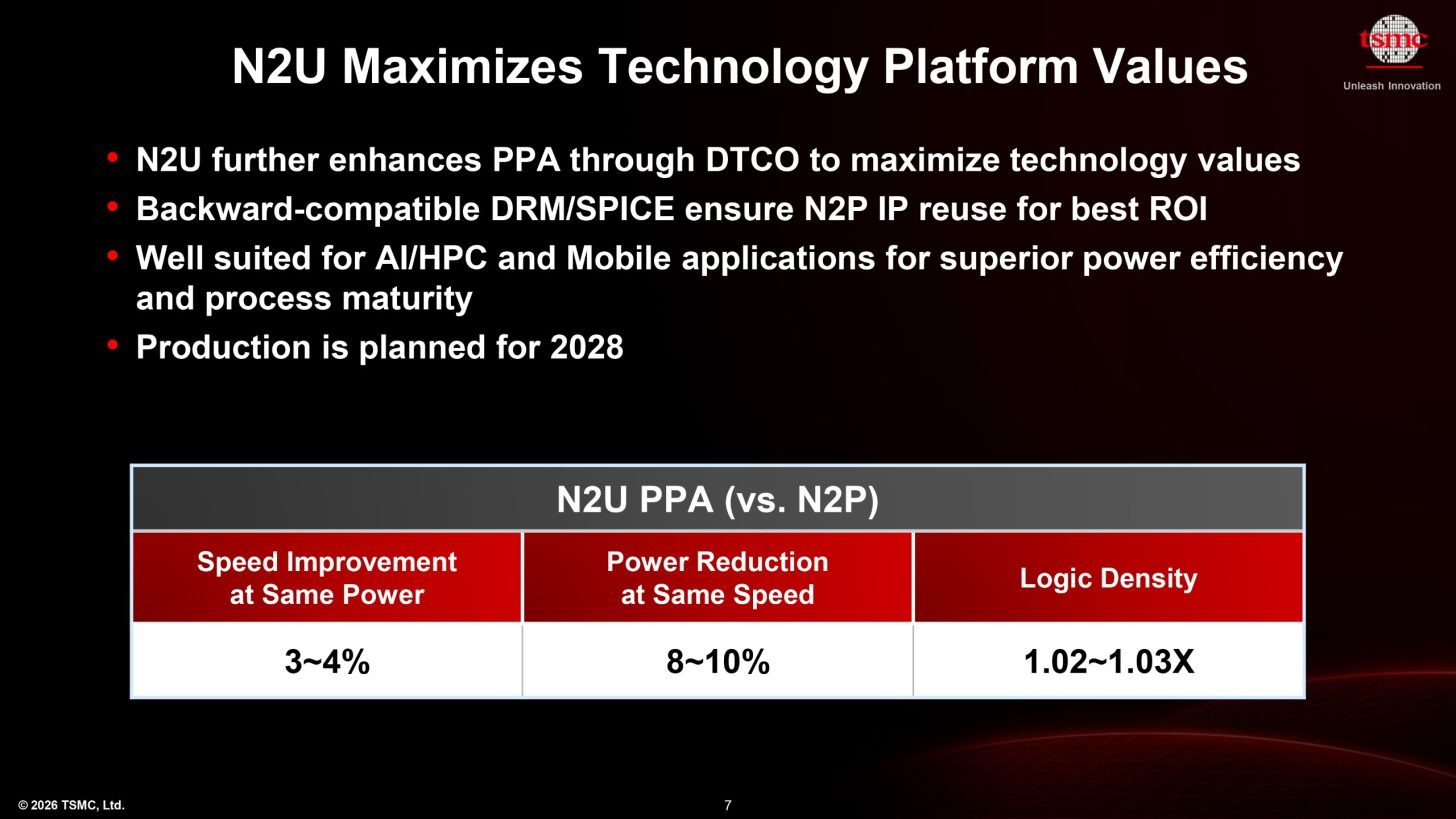
On the 2nm side, TSMC introduced N2U as another extension of the N2 family. The company says N2U offers 3% to 4% speed gains or 8% to 10% lower power at the same performance, along with a 1.02x to 1.03x logic density improvement from N2P. TSMC is pitching N2U as a more balanced option for AI, HPC, and mobile designs that can benefit from the maturity and stronger yield profile of the N2 platform, with production planned for 2028. In practical terms, N2U looks like TSMC’s way of turning N2 into a longer lived platform rather than a one step generational stop.
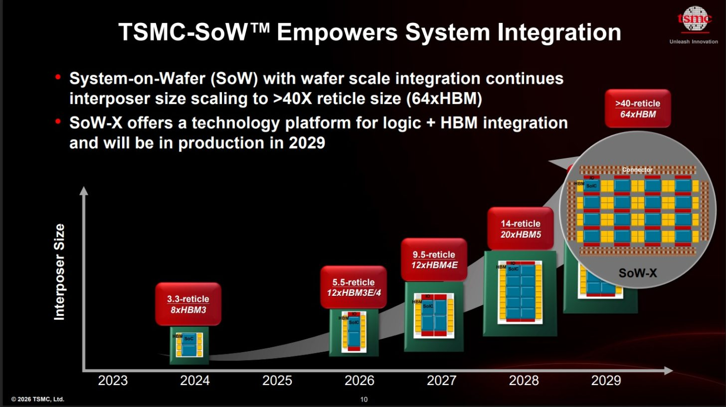
Packaging remains just as important as the transistor roadmap, and TSMC made that very clear. The company says it is already producing 5.5 reticle CoWoS and is planning larger versions, including a 14 reticle CoWoS package capable of integrating about 10 large compute dies and 20 HBM stacks in 2028. Beyond that, TSMC plans to go past 14 reticles in 2029, alongside its 40 reticle SoW X System on Wafer technology. For AI hardware, that may be as important as the logic nodes themselves, because memory capacity and chip integration are increasingly becoming the real limiters in accelerator design.
TSMC also detailed progress around 3D stacking and optics. A14 to A14 SoIC is set for production in 2029 with 1.8x higher die to die I O density than N2 on N2 SoIC, while TSMC COUPE on substrate enters production in 2026 with claimed 2x power efficiency and 10x lower latency versus pluggable optical solutions on the board. Those numbers reinforce how much the future roadmap is about the whole package and interconnect story, not just shrinking transistor dimensions.
The other big takeaway is what TSMC is not doing yet. According to reporting tied to the symposium and earlier TSMC comments, the company does not expect to use High NA EUV through 2029. Kevin Zhang said TSMC will adopt High NA when it provides meaningful and measurable benefit, but that the company’s technology teams are still finding ways to extend the life of current EUV systems while preserving scaling gains. That is a very calculated message. TSMC is not rejecting High NA as a technology, but it is refusing to absorb the huge cost premium before it sees a strong enough return.
From a market perspective, this is classic TSMC execution. The company is pushing multiple fronts at once: incremental node evolution, platform extensions, backside power, larger AI packaging, advanced stacking, and optics, while holding back on High NA EUV until the economics improve. That approach should help customers who want a more predictable roadmap and it also reduces the risk of overinvesting in tools that are still extraordinarily expensive at a time when capital is already being pulled hard by AI fabs and packaging expansion.
For the industry, the message is straightforward. TSMC is still scaling aggressively into 2029, but it is doing so on its own terms. Instead of racing to be first with every lithography tool, it is choosing to maximize what it already has while building out the packaging and power technologies that matter most for the AI era.
Do you think TSMC is making the right move by delaying High NA adoption, or should it be pushing harder on the most advanced lithography sooner?