
Google’s Frozen V2 Could Drop CoWoS by Baking Gemini Architecture Into Silicon
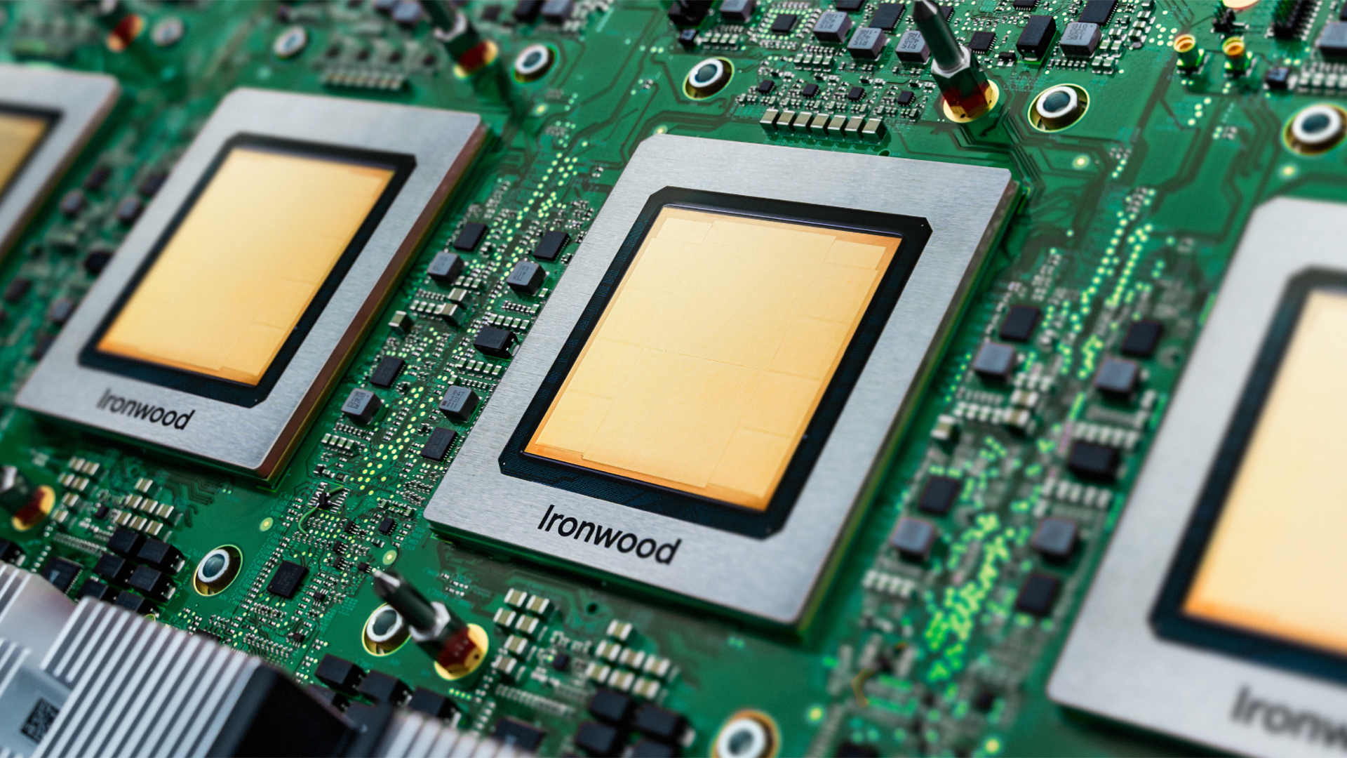
Google is reportedly developing a highly specialized artificial intelligence chip known as Frozen V2, designed to run future Gemini models with substantially greater efficiency while reducing its dependence on expensive High Bandwidth Memory and TSMC’s CoWoS packaging.
According to The Information, Frozen V2 would form a separate branch of Google’s custom silicon portfolio rather than directly replacing its Tensor Processing Units. The project aims to hardwire portions of Gemini’s neural network architecture into the processor while allowing updated model weights to remain programmable.
This distinction is important. Google is not reportedly fixing an entire version of Gemini permanently inside the chip. Instead, the underlying structure used to execute the model would become part of the physical silicon, reducing the scheduling, data movement, and general purpose calculations normally required when running artificial intelligence software on a more flexible accelerator.
Google engineers reportedly estimate that Frozen V2 could process between 6 and 10 times more tokens per watt than the company’s latest TPU technology. Deployment could begin during 2028, although the architecture remains under development and Google may initially treat the project as a limited experiment rather than producing it at normal TPU volumes.
A separate Morgan Stanley research note describes Frozen V2 as an SRAM focused inference architecture that could enter limited production during 2027 before expanding during 2028. The analysts believe Marvell could become a development partner, although neither Google nor Marvell has confirmed an agreement for the project.
The SRAM description requires additional context. Modern processors already integrate SRAM directly into their silicon for caches and fast local memory. The potential change with Frozen V2 would be using a much larger SRAM centered architecture to retain more frequently accessed model data close to the compute engines, potentially reducing or removing the requirement for external HBM.
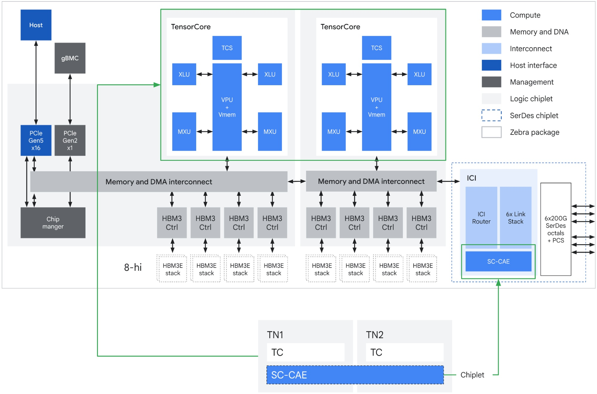
Without multiple HBM stacks, Frozen V2 may also avoid TSMC’s CoWoS advanced packaging technology. CoWoS is widely used to connect large AI processors with HBM through high density interposers, but it remains expensive, capacity constrained, and complex to manufacture. An inference chip relying primarily on internal SRAM could use a simpler package while lowering power consumption associated with moving data between compute silicon and external memory.
Google’s current TPU roadmap is moving in a different but complementary direction. The company’s TPU 8i includes 384MB of on chip SRAM, 288GB of HBM, and 19.2Tbps of interconnect bandwidth to support agentic inference and reinforcement learning. Reported future designs such as TPUv9 Triggerfish could expand SRAM further while introducing HBM4E and a dedicated management die.
Frozen V2 would therefore not make conventional TPUs obsolete. TPUs would retain the flexibility required for training, multiple model families, and rapidly changing workloads, while Frozen V2 could serve enormous volumes of predictable Gemini inference requests at a lower cost.
The concept resembles the wider movement toward hardcoded artificial intelligence accelerators. Taalas places model weights inside Mask ROM and uses SRAM for dynamic information, eliminating HBM and CoWoS while achieving high inference throughput. Frozen V2 is reportedly less restrictive because it would freeze the Gemini architecture rather than its exact trained weights, allowing Google to deploy updated models as long as their underlying structure remains compatible.
That flexibility still has limits. If Google significantly changes Gemini’s architecture, introduces new attention mechanisms, or restructures how the model activates experts, Frozen V2 silicon could become obsolete. The company would then need to redesign and manufacture another processor, making the strategy most practical when model architectures remain stable and deployment volumes are large enough to recover development costs.
Frozen V2 represents Google pushing hardware and software integration beyond the traditional custom accelerator model. Instead of creating another processor capable of running many artificial intelligence workloads, Google appears interested in designing silicon around the specific structure of Gemini.
The potential reward is enormous. Google operates enough Gemini inference traffic to justify specialized hardware that saves power, packaging capacity, and operating costs on every generated token. Even modest efficiency gains could translate into substantial savings across its global data center infrastructure.
However, Frozen V2 is also a calculated bet that Gemini’s fundamental architecture is beginning to stabilize. Freezing too much of the model into silicon could deliver exceptional efficiency today while limiting Google’s ability to adopt a major architectural breakthrough tomorrow.
Could model specific chips such as Frozen V2 eventually become more important for AI inference than flexible GPUs and TPUs?
