
China Develops First 3.5D Infinity Chiplet and 3D DRAM AI Architecture to Reduce HBM Dependence
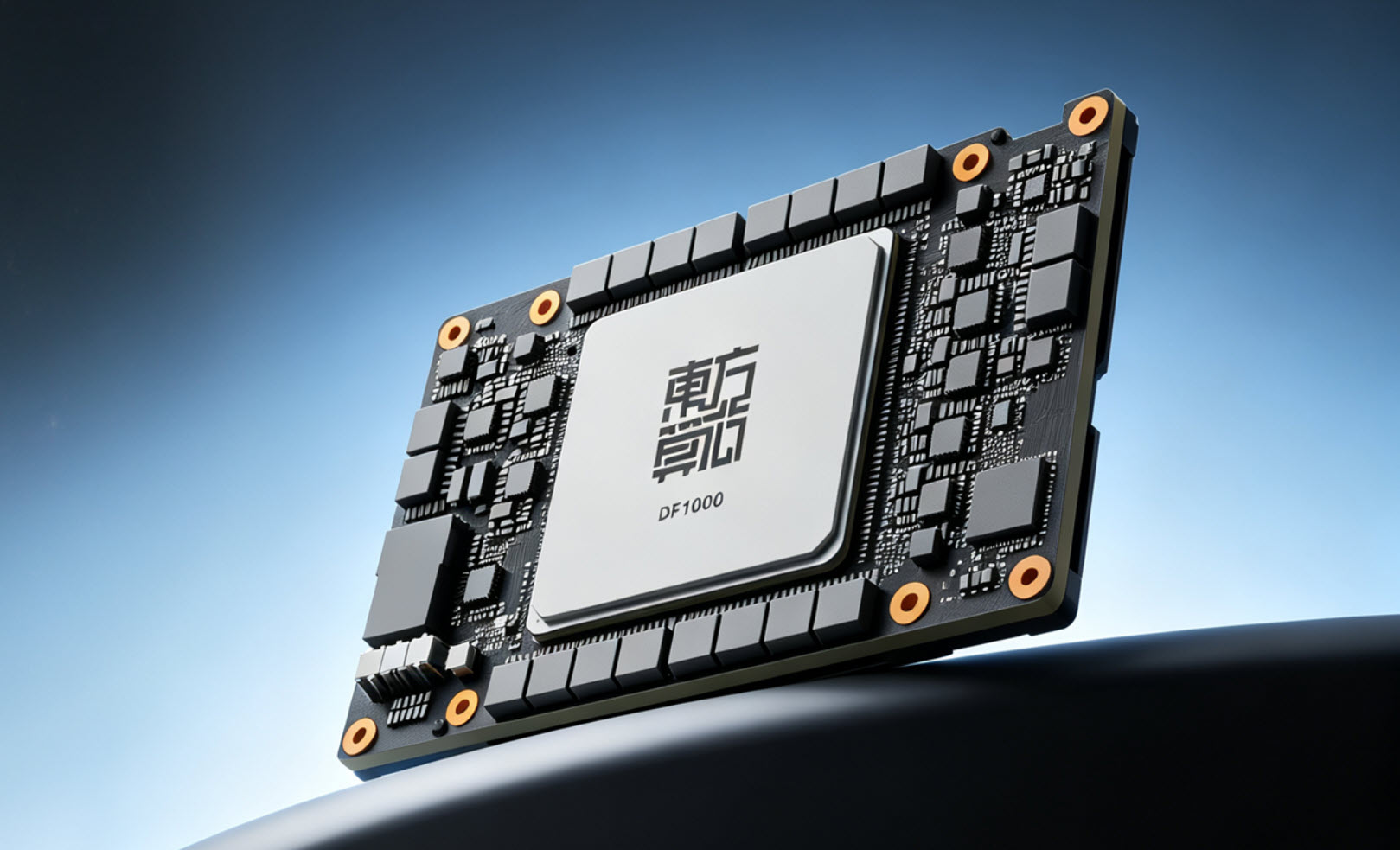
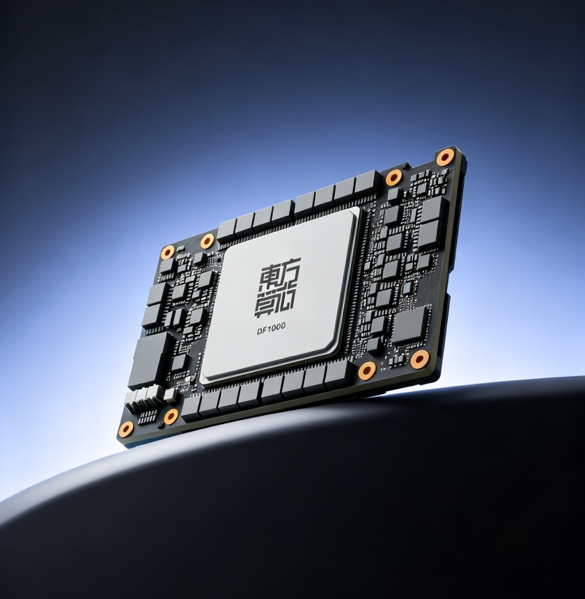
Chinese semiconductor company DFSX has introduced the DF1000, an artificial intelligence accelerator built around software defined computing, near memory processing, and vertically stacked 3D DRAM. The company is also developing an Infinity Chiplet 3.5D+ packaging architecture designed to scale future processors without relying on imported high bandwidth memory or the most advanced semiconductor manufacturing processes.
The DF1000 was presented during a DFSX technology and product event held in Shanghai on July 13, 2026. According to EET China, DFSX describes it as the first software defined computing chip to combine logic and memory through a domestic 3D integrated architecture. The accelerator is manufactured using a mature 14 nm process and is reportedly supported by a supply chain located entirely within China.
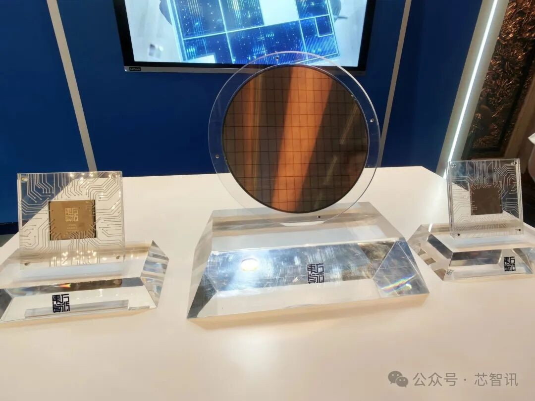
The official DFSX DF1000 product page identifies the accelerator as a platform for large language model training and inference. It follows the OAM 2.0 specification, allowing it to integrate with compatible artificial intelligence servers from Chinese original equipment manufacturers. DFSX is also developing its own software stack and distributed execution environment to reduce dependence on foreign accelerator ecosystems.
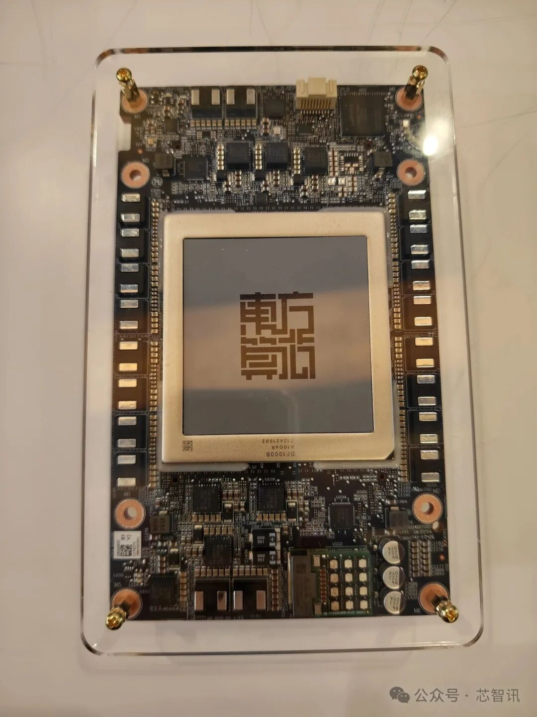
At the silicon level, DF1000 delivers a claimed 520 TFLOPS of BF16 compute performance, 6.4 TB/s of memory bandwidth, and 900 GB/s of Scale up interconnect bandwidth. Its primary differentiator is the use of 3D DRAM positioned directly above the logic architecture rather than external HBM packages placed beside the compute processor.
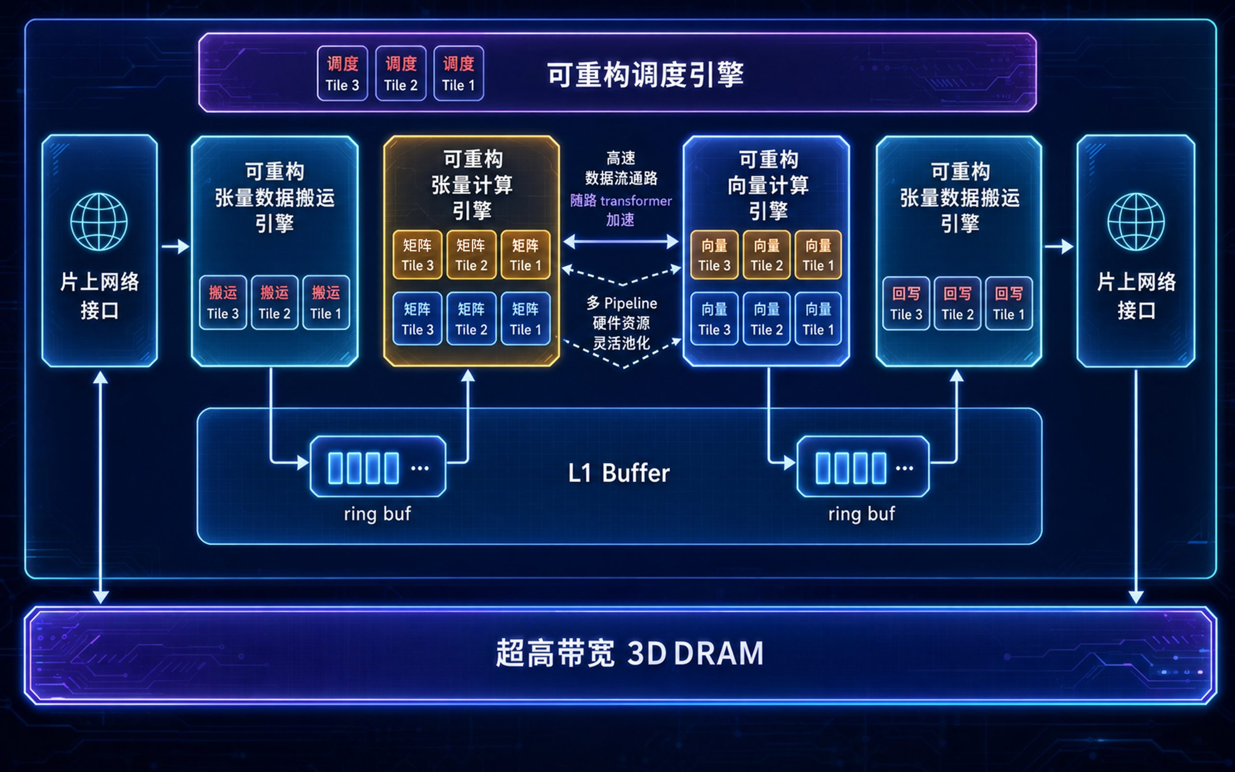
DFSX uses hybrid bonding to connect the logic and memory layers without conventional microbumps. The company says this reduces the connection pitch from tens of micrometers to below 1 micrometer, increasing interconnect density and bandwidth density while reducing the energy required to move data between compute and memory.
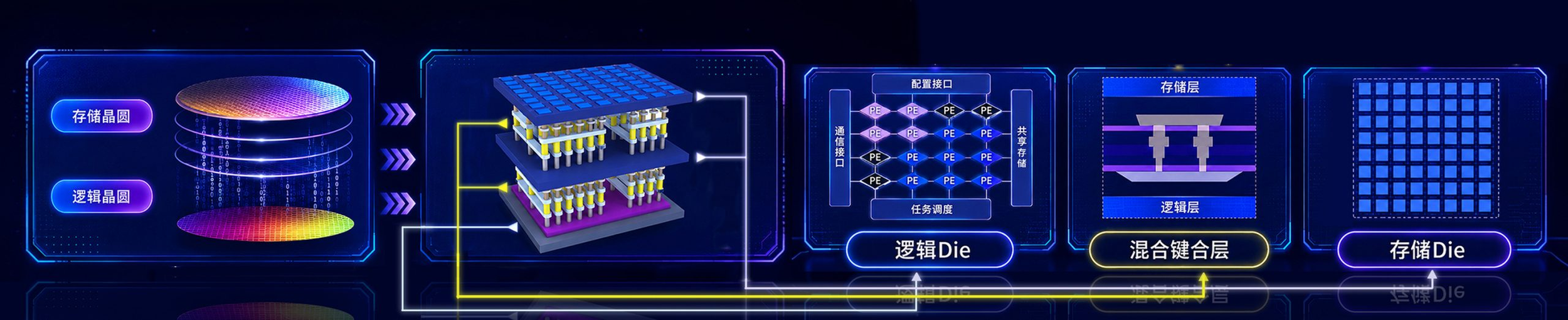
According to DFSX, the architecture can provide dozens of times more through silicon connections than conventional HBM structures and more than 5 times the bandwidth at an equivalent memory capacity. Additional DRAM wafers can theoretically be stacked to increase capacity, although greater stacking complexity may also create challenges involving manufacturing yield, thermal management, repairability, and production cost.
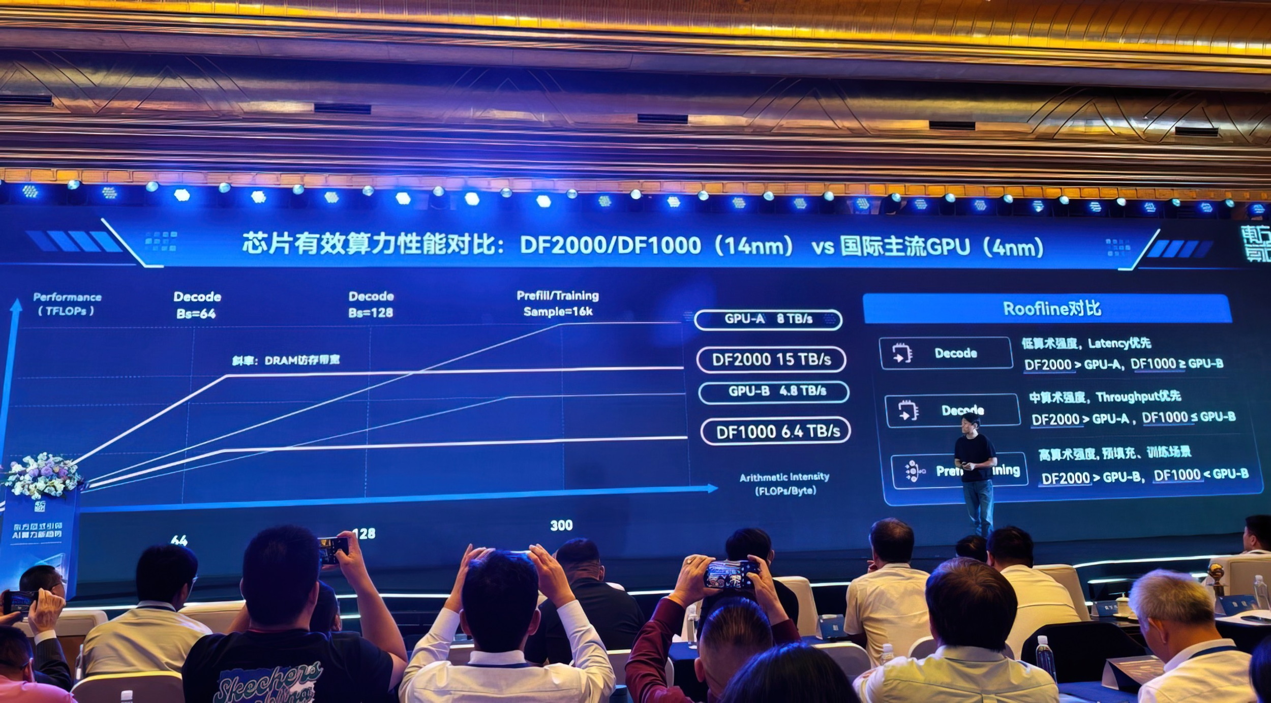
The 6.4 TB/s memory bandwidth claimed for DF1000 is nearly twice the bandwidth of an NVIDIA H100 and approximately 33% greater than an H200. However, memory bandwidth should not be treated as a direct measurement of overall accelerator performance. DFSX’s own presentation indicates that DF1000 provides approximately 52.6% of the raw compute performance available from NVIDIA’s Hopper generation H100 and H200 processors.
This suggests that the DF1000 could be particularly competitive in memory constrained inference workloads where token generation, model capacity, and data movement are more important than maximum arithmetic throughput. In workloads with greater computational intensity, its lower raw processing performance may remain a significant limitation.
DFSX reported throughput reaching 500 tokens per second with the Llama 3 70B model. The company also recorded a 10 ms decode time per output token with Step 3.7 Flash and 20 ms with DeepSeek 3.2 using its AFD distributed inference architecture. These figures come from internal testing and have not yet been validated through independent benchmarks, standardized model configurations, or direct testing against comparable NVIDIA systems.
The arrival of DF1000 comes as access to advanced foreign artificial intelligence processors remains heavily controlled. Select NVIDIA H200 shipments have begun reaching approved Chinese customers under a licensing program, but supply remains limited and subject to government approval, product testing, and customer verification.
DFSX is positioning 3D DRAM as a domestic alternative to this uncertain HBM supply chain. Rather than attempting to reproduce the same processor, memory, and packaging structure used by NVIDIA and AMD, the company is reorganizing the relationship between compute and memory around technologies that can be manufactured using mature domestic processes.
Its next major development is Infinity Chiplet 3.5D+, a multi chip package intended to combine several computing dies with vertically integrated 3D DRAM. The architecture uses 3.5D stacking to replace conventional data storage structures, reducing the package area occupied by memory while increasing the space available for additional computing resources.
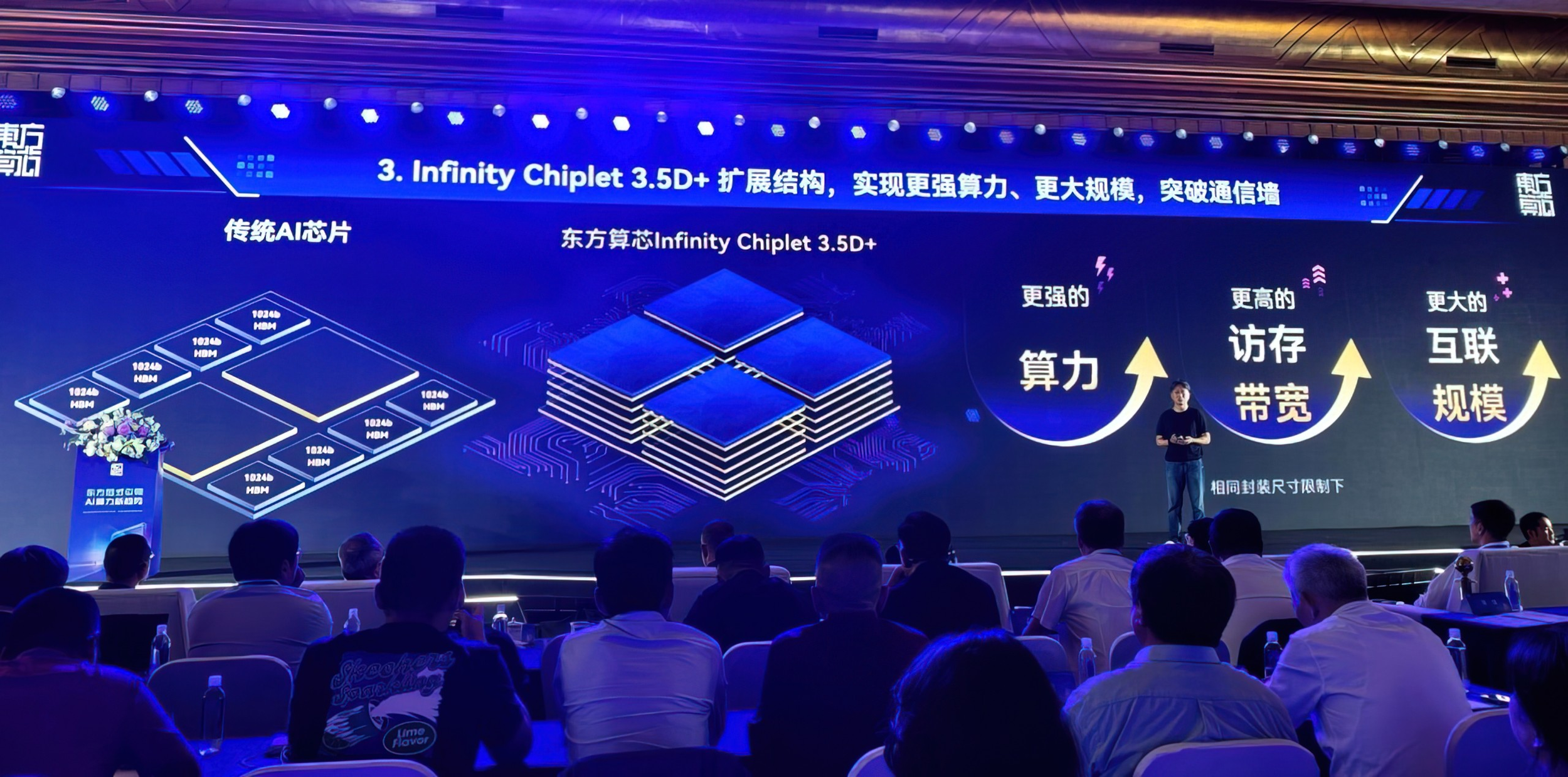
Removing external HBM packages also allows more of the processor’s input and output area to be assigned to chip interconnects. DFSX says this could provide greater Scale up bandwidth and allow more compute chiplets to operate within the same package dimensions. Compared with conventional 2.5D packaging, the company claims Infinity Chiplet can deliver greater compute density, memory bandwidth, and interconnect capacity without requiring a leading edge manufacturing node.
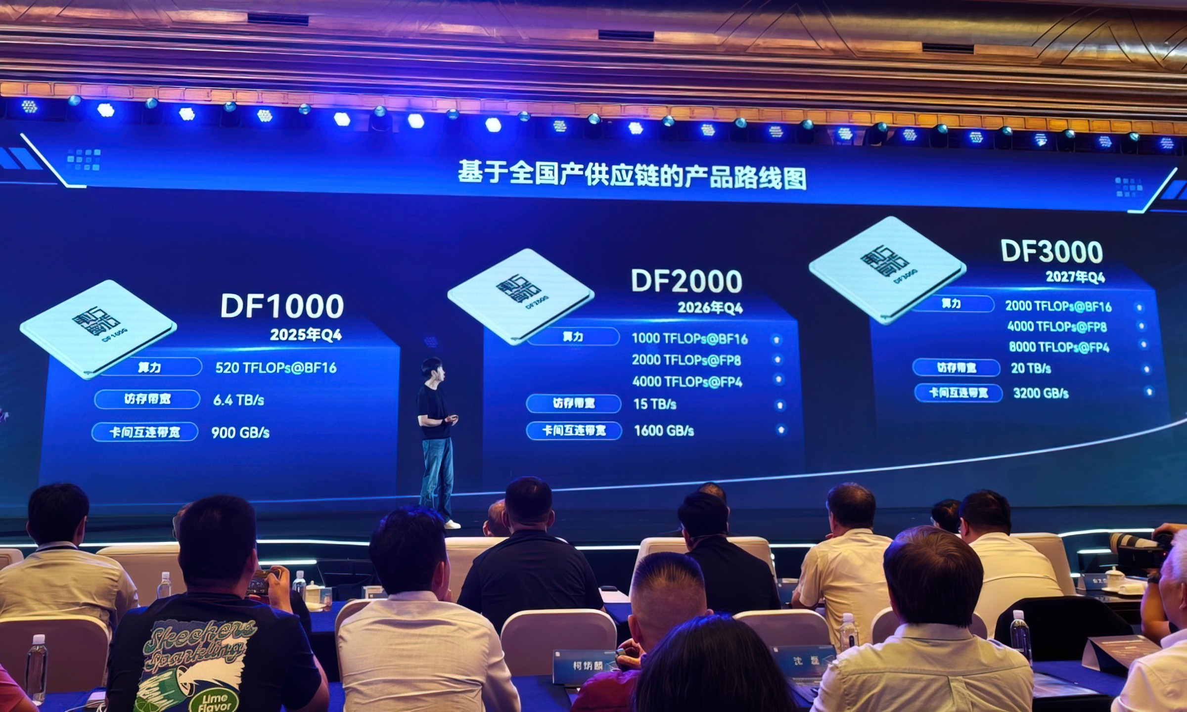
The company has already announced an aggressive product roadmap. DF2000 is scheduled for Q4 2026 and will continue using a 14 nm manufacturing process. It is expected to provide 1000 TFLOPS of BF16 performance, 2000 TFLOPS of FP8, 4000 TFLOPS of FP4, 15 TB/s of memory bandwidth, and 1600 GB/s of Scale up interconnect bandwidth.
DFSX claims DF2000 will exceed NVIDIA Hopper products across several technical measurements and could reach Blackwell class performance in workloads that benefit heavily from memory bandwidth. These projections remain targets until production silicon becomes available and can be evaluated using comparable power limits, software environments, model configurations, and system costs.
DF3000 is planned for Q4 2027 with 2000 TFLOPS of BF16 compute, 4000 TFLOPS of FP8, 8000 TFLOPS of FP4, 20 TB/s of memory bandwidth, and 3200 GB/s of Scale up connectivity. DFSX intends for the third generation processor to compete more directly with NVIDIA’s Blackwell platform, although the company has not yet confirmed whether DF3000 will remain on 14 nm or transition to another process.
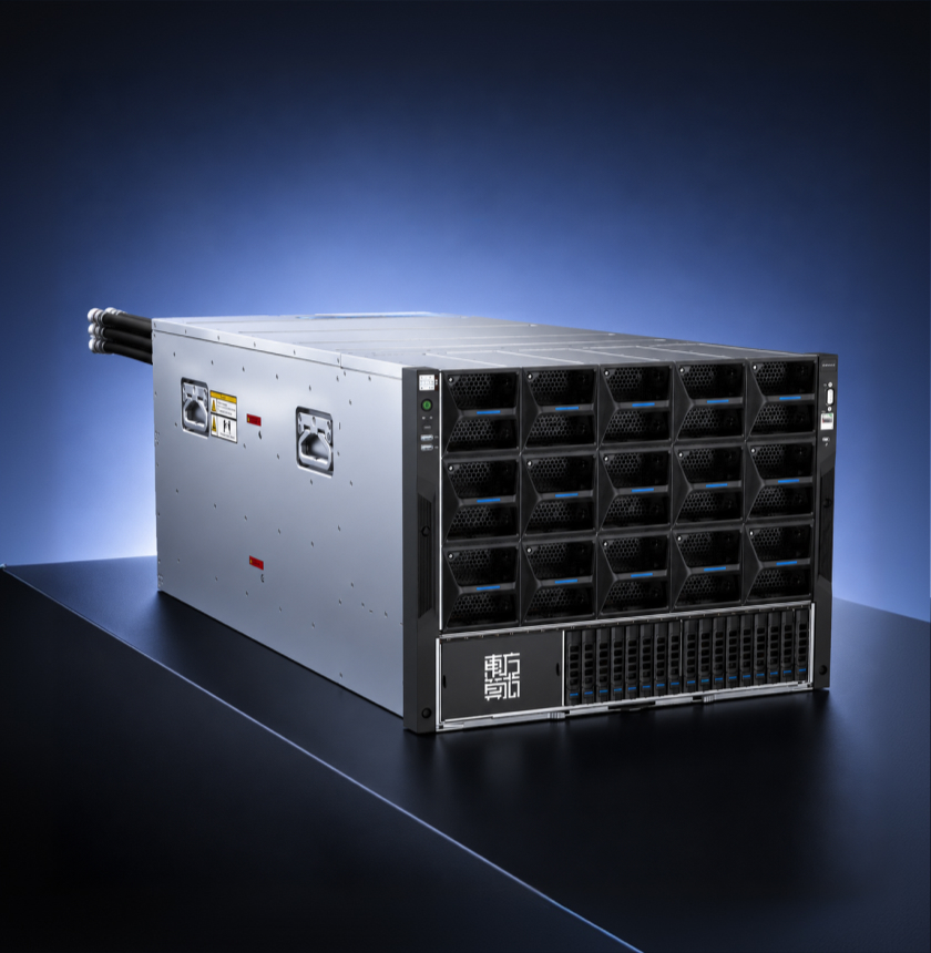
DF1000 is also being expanded beyond individual accelerator cards. An 8 accelerator module provides a claimed 4.16 PFLOPS of BF16 performance, 51.2 TB/s of combined memory bandwidth, 7.2 TB/s of Scale up connectivity, and 120 CPU cores within a reported 12 kW power envelope.
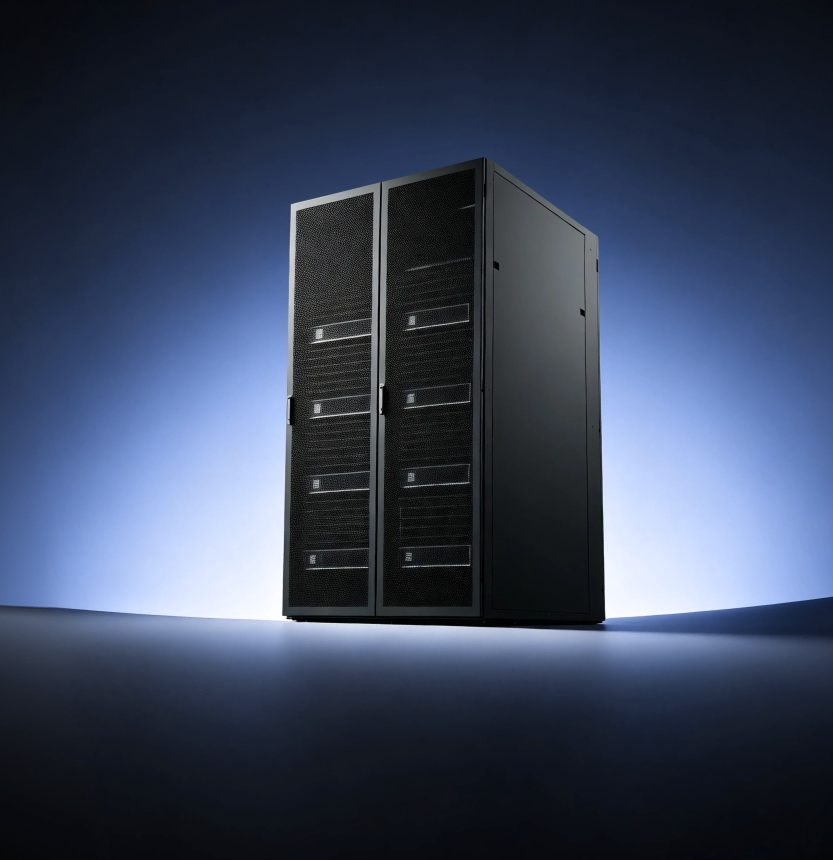
DFSX has also presented the TY64 supernode with 64 DF1000 accelerators, alongside QY100 servers and HS128 and HS512 cluster configurations. These systems combine DFSX hardware with its CAAP software environment and support domestic processors, operating systems, and mainstream artificial intelligence frameworks.
The DF1000 is important not because it immediately replaces NVIDIA’s fastest accelerators, but because it demonstrates how Chinese companies are redesigning artificial intelligence hardware around the resources available within their domestic supply chain.
Its 14 nm process places it several generations behind leading international processors, while DFSX’s performance claims still require independent testing. Packaging yield could also become a major obstacle because every additional logic and memory layer increases manufacturing complexity and reduces the percentage of fully functional finished chips.
However, the company’s decision to prioritize memory proximity, bandwidth, chiplet scaling, and software defined execution represents a credible strategic response to restricted access to advanced fabrication and HBM. In artificial intelligence inference, where memory movement can determine real performance as much as raw compute, architectural efficiency may allow mature process technology to remain commercially relevant.
The defining challenge will be execution. DFSX must prove that 3D DRAM can be manufactured reliably at scale, that its software stack can support modern models without extensive redevelopment, and that its systems can provide competitive performance per watt and total ownership cost. If it succeeds, Infinity Chiplet could become more than an alternative packaging method. It could establish a separate development path for China’s artificial intelligence infrastructure.
Can 3D DRAM and mature process chiplets become a practical alternative to HBM, or will manufacturing yield and software support prevent DFSX from competing with NVIDIA?
