
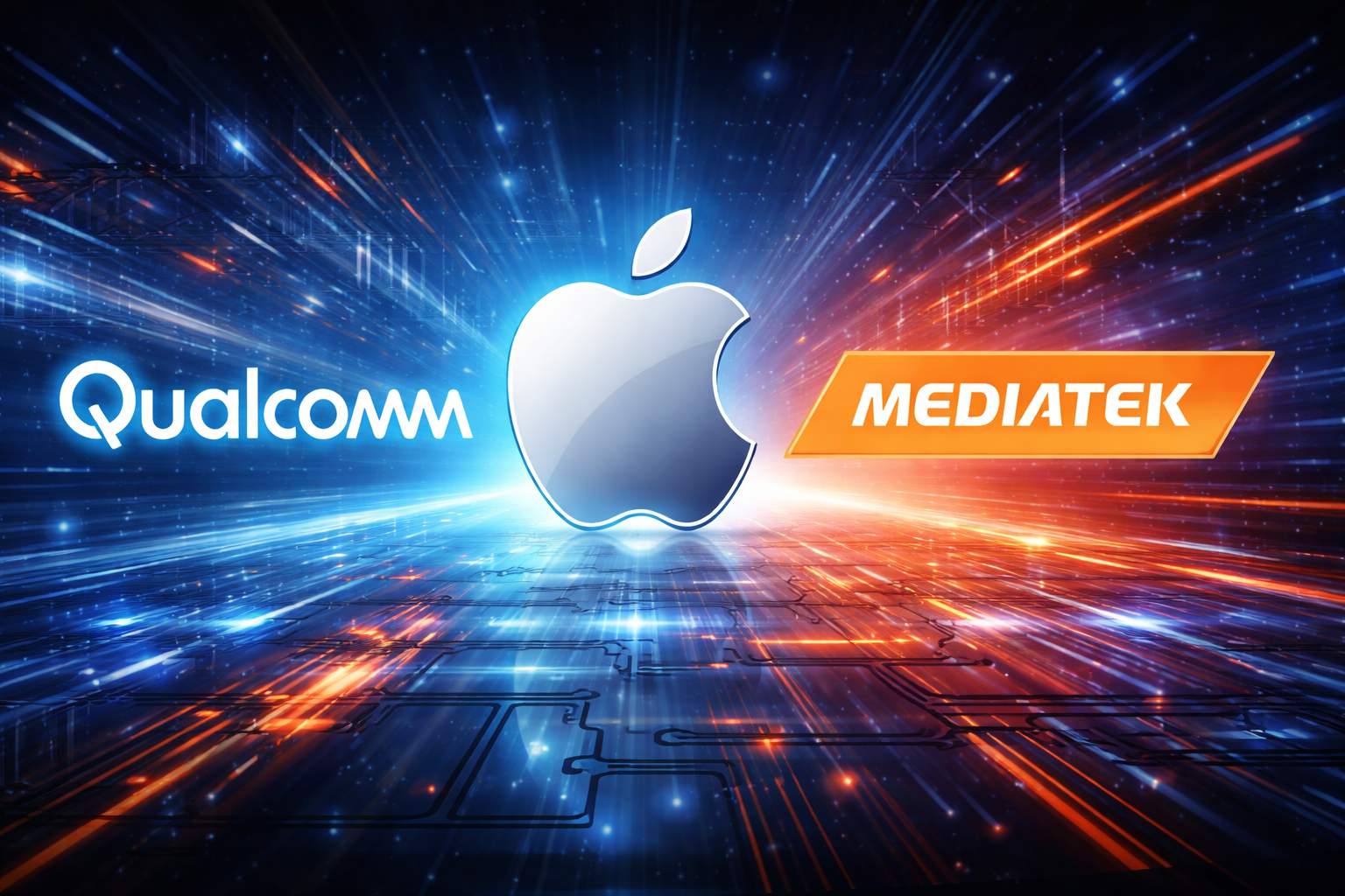
TSMC’s Advanced Nodes Are Pushing Smartphone SoCs Toward the 5GHz Era
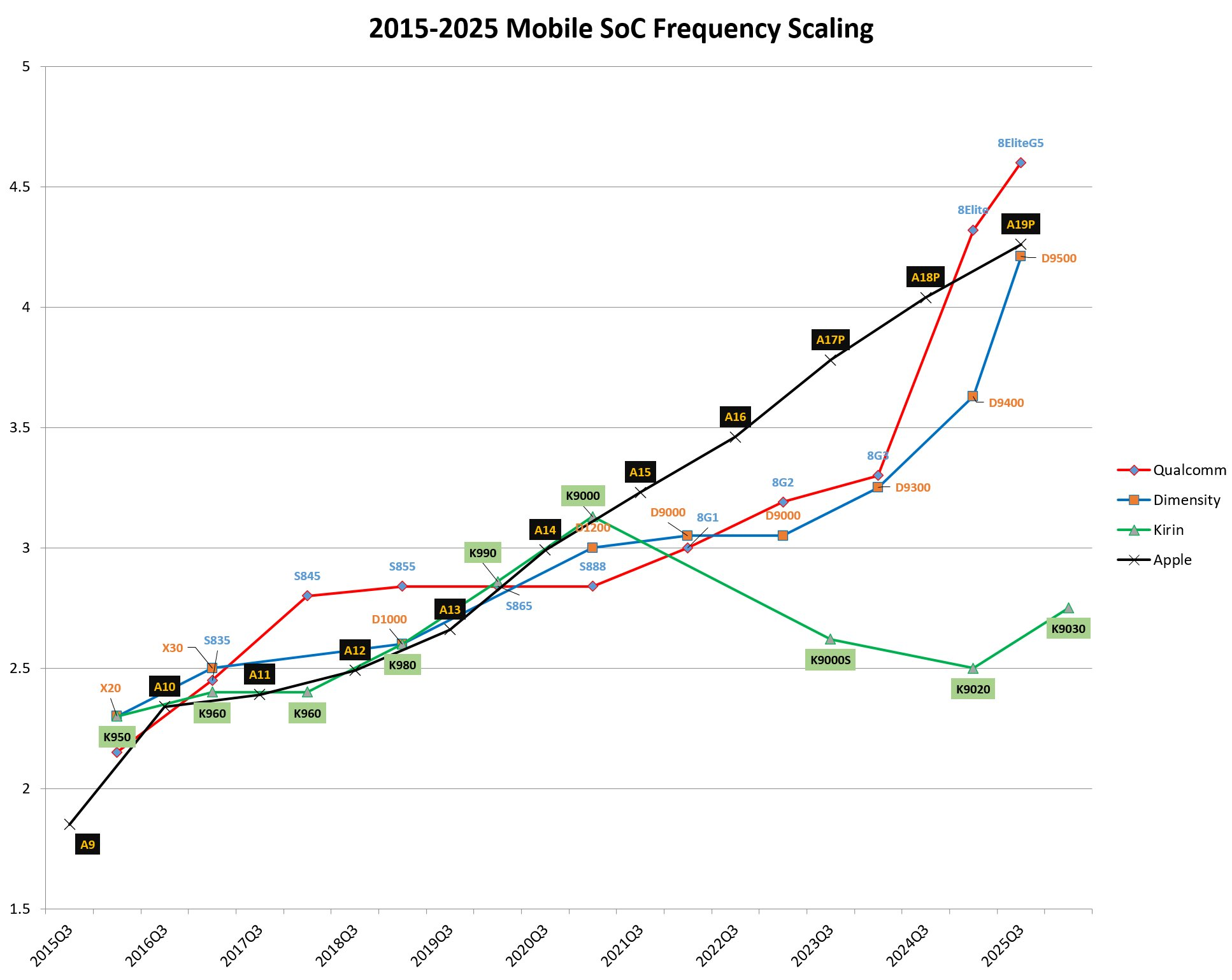
The next wave of flagship smartphone silicon is shaping up to hit a milestone that would have sounded unrealistic not that long ago. According to a chart shared by Kurnal and recent supply chain reporting, Apple, Qualcomm, and MediaTek are all moving toward significantly higher CPU clocks on their premium mobile chips, with upcoming designs rumored to approach or even touch 5.00GHz for the first time in the smartphone market. That trend is closely tied to TSMC’s continued lead in advanced manufacturing, especially as 2nm era products begin entering the conversation for late 2026.
The broader pattern is easy to see. Qualcomm’s current top tier mobile silicon has already pushed well past the older ceiling that flagship smartphone chips used to sit under, and new rumors around the next generation suggest the company is targeting 5.00GHz territory with a future Snapdragon flagship. MediaTek is being linked to a similar ambition with its upcoming Dimensity 9600 Pro, while Apple’s next Pro class iPhone chip is also expected to continue climbing in frequency, though still below that 5.00GHz mark based on current leaks. None of those clock targets are officially finalized yet, but the direction of travel is clear: mobile flagship SoCs are now chasing frequencies that were once associated far more with desktop CPUs than phones.
TSMC’s role in that shift is hard to overstate. The company remains the dominant advanced foundry for premium smartphone SoCs, and market reports continue to point to Apple, Qualcomm, and MediaTek all relying on TSMC’s leading nodes for their highest end launches. More specifically, industry reporting has repeatedly tied late 2026 flagship chips from Apple, Qualcomm, and MediaTek to TSMC’s 2nm generation, including N2 and N2P class production paths. That does not mean lithography alone creates performance, but it does provide the transistor efficiency and density needed to make these kinds of clock increases more realistic without power and heat spiraling completely out of control.
That contrast is especially sharp when you look at Huawei. Current reporting around the latest Kirin generation says Huawei still has not pushed its flagship mobile chip past the 3.00GHz barrier, a much lower ceiling than what rivals are now targeting. The most commonly cited reason is not simply architecture, but manufacturing access. Huawei lost access to TSMC’s most advanced production after US export controls tightened, and multiple reports note that the company has been relying on SMIC and older process technology instead. SMIC has been widely associated with 7nm class production using DUV rather than newer EUV lithography, which severely limits how aggressively Huawei can scale frequency and efficiency relative to TSMC fabricated rivals.
That does not make Huawei’s situation purely a technology failure of its own making. The company’s manufacturing constraints are clearly tied to geopolitics and export controls as much as to execution. Since 2019, the United States has imposed increasingly restrictive measures on Huawei’s semiconductor access, and reporting from research and policy sources continues to show that these controls significantly affected Huawei’s ability to use top tier foundry partners such as TSMC. In practical terms, that means Apple, Qualcomm, and MediaTek are racing forward with leading edge TSMC nodes while Huawei is being forced to compete under much tighter manufacturing limits.
Still, raw frequency should not be mistaken for effortless performance. Even if 5.00GHz smartphones arrive this year or next, that does not mean they will hold those speeds for long stretches. In mobile silicon, peak frequency is only part of the story. Sustained clocks, thermal throttling, power efficiency, and device level cooling all matter just as much. We are already seeing this issue show up in recent rumors around future flagship SoCs, where extremely high target frequencies are being discussed alongside concerns about heat and short burst behavior rather than fully sustained operation. That means TSMC’s manufacturing advances are enabling the milestone, but physics will still determine how often users really experience it.

This is where smartphone design becomes just as important as the chip itself. Better vapor chambers, improved thermal materials, and more aggressive cooling layouts can help next generation devices sustain performance longer, but there is no escaping the fact that a phone remains a very small thermal envelope compared with a laptop or desktop. So while “5.00GHz smartphone SoC” is a powerful headline and a real technical milestone, the more meaningful question for buyers will be how well these chips translate that peak capability into stable gaming, AI, imaging, and multitasking performance over time. That final point is an inference based on current mobile chip trends and the reported thermal concerns around upcoming flagship SoCs.
In strategic terms, though, TSMC is the clear winner in this part of the industry story. As long as Apple, Qualcomm, and MediaTek keep scaling performance through access to the most advanced nodes, TSMC remains one of the biggest reasons why flagship smartphones continue closing the gap with more traditional computing devices in certain workloads. The 5.00GHz milestone may belong to the chip brands on the box, but the foundry behind them is still doing a huge part of the heavy lifting.
What do you think matters more for next generation smartphone chips: hitting 5.00GHz on paper, or delivering stronger sustained performance without aggressive throttling?