
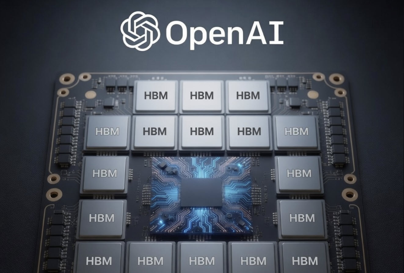
OpenAI Patent Outlines AI Chip Design With Up to 20 HBM Stacks, Pointing to a Bigger Packaging Play Beyond Today’s Limits
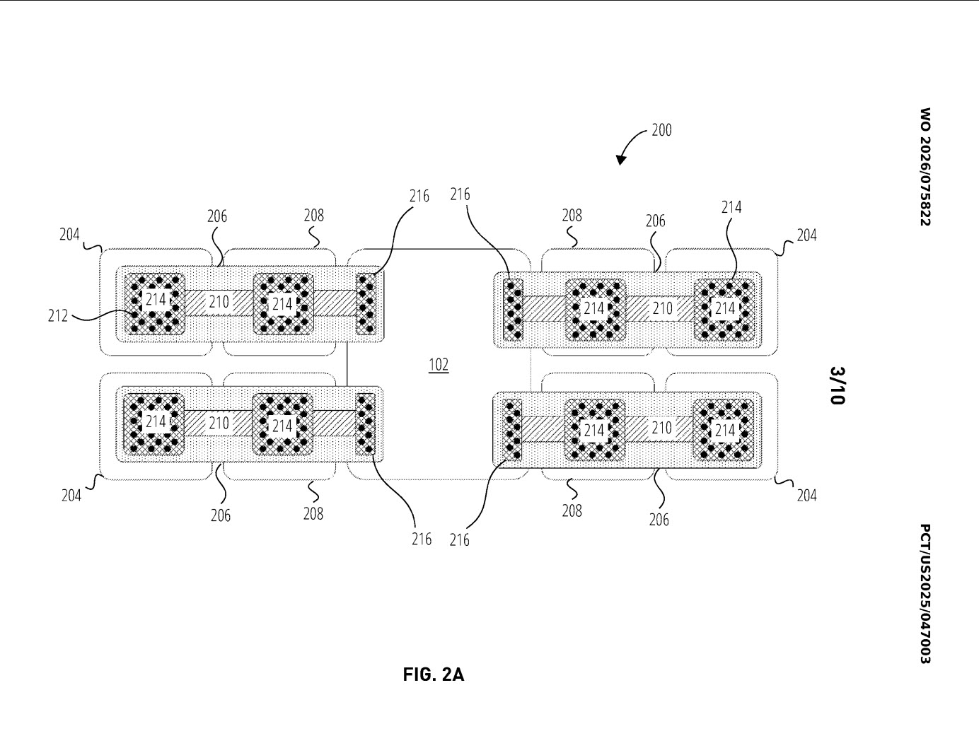
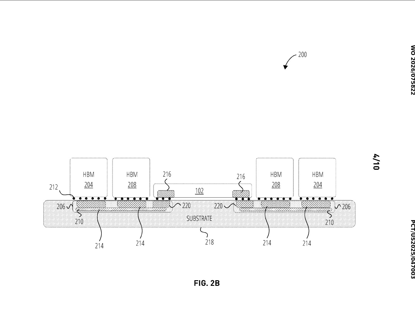
OpenAI has published a new international patent application that sketches out an aggressive future AI packaging concept centered on compute chiplets, I/O chiplets, and a very large number of HBM memory stacks connected through embedded logic bridges. The patent, titled Non Adjacent Connection of High Bandwidth Memory Chiplets, I O Chiplets, And Compute Chiplets Through Embedded Logic Bridges, describes an architecture designed to overcome the physical distance limits that normally constrain how HBM is placed around compute silicon in advanced packages.
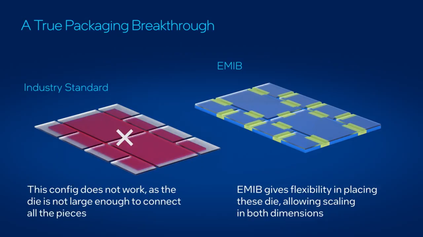
At the core of the concept is a simple but important idea. Instead of relying only on direct adjacency between the compute chiplet and HBM stacks, OpenAI’s patent proposes using embedded logic bridges to extend that communication path and maintain high speed die to die connectivity. According to the patent summary cited in coverage of the filing, the design is meant to push communication beyond the roughly 6 mm limit imposed by current HBM placement constraints, allowing memory to be positioned farther away while still remaining part of a high performance package.
That matters because memory proximity has become one of the biggest bottlenecks in large AI accelerators. Modern AI chips need massive bandwidth and capacity, but advanced package layouts can only fit so many HBM stacks next to a compute die before routing, area, thermals, and reticle related limits start to push back. OpenAI’s proposed bridge based structure is aimed directly at that problem, and it also aligns with the broader chiplet trend now spreading across AI and high performance computing. The UCIe consortium describes its standard as an open package level die to die interconnect intended to let chiplets mix and match within larger systems on package, including designs that exceed normal reticle size limitations.
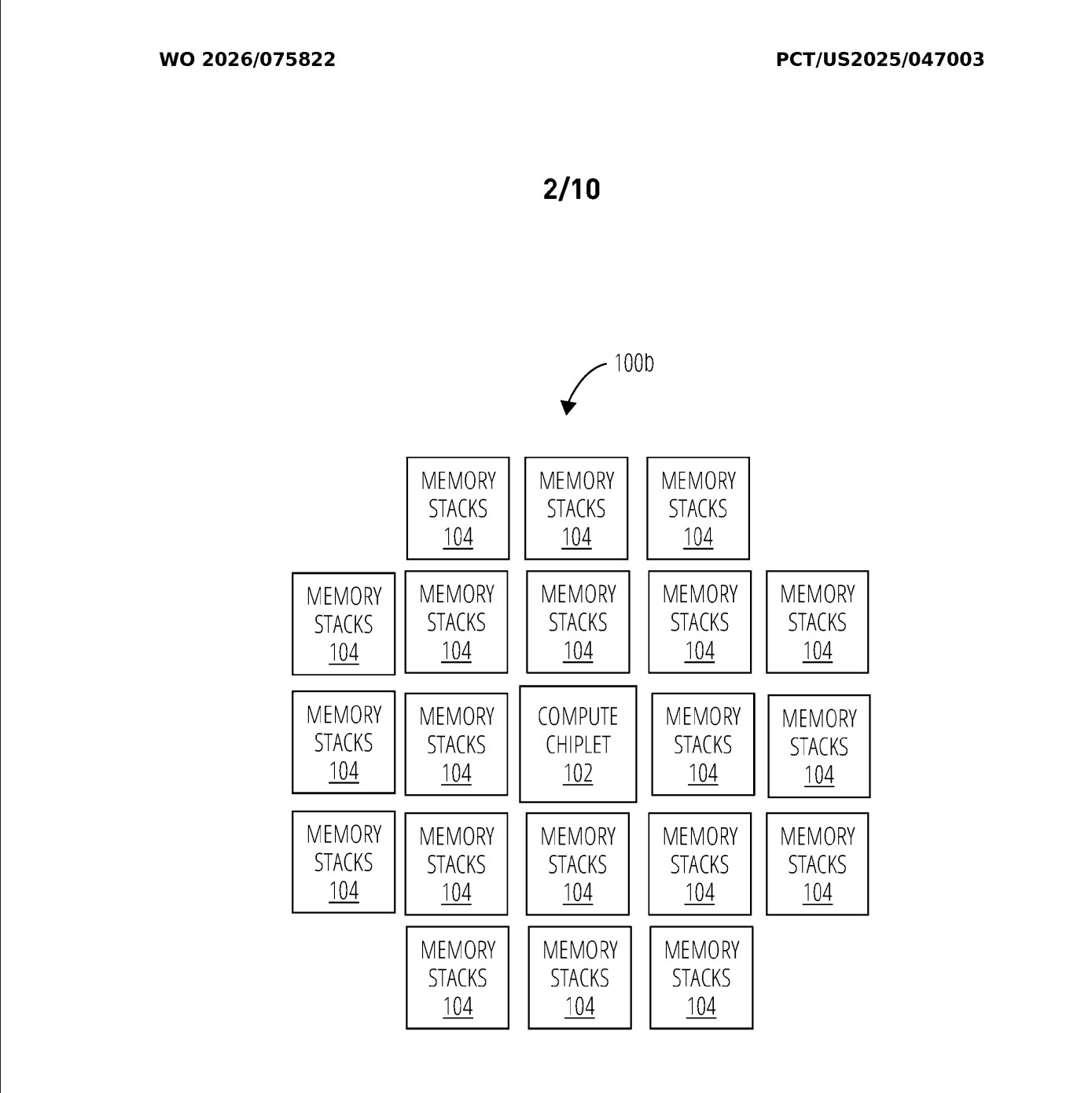
One of the most eye catching parts of the patent is an example configuration showing a compute chiplet surrounded by as many as 20 HBM stacks. That is far beyond the 4, 6, or 8 stack layouts most people currently associate with mainstream advanced AI package discussions, which is exactly why the filing has attracted so much attention online. The patent’s visual examples have already started circulating through the hardware community, including via SETI Park on X, because they suggest a future design philosophy where memory scaling inside the package becomes much more aggressive than what is common today.
The bridge concept also explains why observers immediately started comparing the idea to Intel’s EMIB approach. Intel describes EMIB as an embedded bridge technology that enables high bandwidth connectivity between multiple large chiplets without requiring a full silicon interposer, and says it is specifically meant to help scale package flexibility and total silicon area in advanced systems. That does not mean OpenAI is confirmed to be using Intel technology, and the patent itself does not establish a partnership or foundry decision. But as a technical analogy, the comparison is reasonable because both approaches revolve around embedded bridge structures that extend how dies can be connected inside a package.
That distinction is important. A patent is not a product announcement, and it is not proof that OpenAI will manufacture this exact chip. What it does reveal is where OpenAI’s engineering and research interest appears to be heading. The company is thinking seriously about package level memory expansion, standardized die to die communication, and ways to break through current HBM adjacency constraints for future AI workloads. In practical terms, that suggests OpenAI is exploring the same kinds of system level bottlenecks that already define the AI hardware race: bandwidth density, package area, power efficiency, and cost effective scaling.
There is also a bigger industry signal here. If more AI companies move toward architectures that rely on far more HBM per package, that could intensify pressure across the memory supply chain even further. The AI market is already heavily constrained by advanced packaging and high bandwidth memory availability, so a future where custom accelerators aim for dramatically larger HBM footprints would only raise the stakes for suppliers and packaging partners. OpenAI’s patent does not prove that future demand spike by itself, but it clearly shows the direction of travel: more memory, more chiplets, more bridge logic, and much larger integrated AI packages.
From a strategy perspective, this filing fits the broader pattern now shaping the AI infrastructure market. Competitive advantage is no longer just about the raw compute die. It is about how much memory can be attached, how efficiently chiplets can communicate, and how far package architecture can scale before costs and physics push back. OpenAI’s patent suggests the company does not want to stay limited by today’s conventional HBM layouts, and that alone makes this a meaningful document to watch even if the final commercial form ends up looking different.
If this kind of packaging ever reaches production, it could point to a future where AI accelerators are defined just as much by memory architecture as by compute itself.
Do you think the next big AI chip battle will be won by raw compute, or by whoever finds the smartest way to pack in more HBM without breaking cost and power limits?