
Intel Foundry Unveils the World’s Thinnest GaN Chiplet at Just 19μm, Targeting Next Generation Data Center and Wireless Power Designs
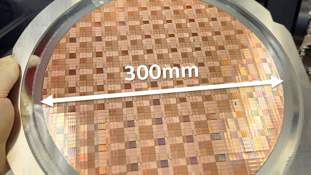
Intel Foundry has announced a major semiconductor research milestone with what it says is the world’s thinnest gallium nitride chiplet, built on a 300 mm GaN on silicon wafer and measuring just 19 μm at its silicon base. According to Intel, the new chiplet was presented at the 2025 IEEE International Electron Devices Meeting and is designed to push higher power, faster switching, and better efficiency into a much smaller footprint for future compute, networking, and communications hardware.
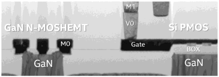
The significance of this work goes beyond simple thinness. Intel says its researchers not only harvested this ultra thin GaN chiplet from a 300 mm wafer, but also successfully integrated GaN transistors with traditional silicon based digital control circuits on the same chip. That matters because it removes the need for a separate companion chiplet for control logic, which can reduce routing overhead, save space, and improve power efficiency in dense system designs.
Intel frames this as an important step for the next generation of data centers, graphics processors, servers, and 5G and 6G infrastructure, all of which are demanding more performance in increasingly constrained thermal and physical envelopes. In the company’s explanation, the combination of an ultra thin GaN base and monolithic on die digital control circuits creates a more compact and potentially more efficient building block for future chiplet based systems.
One of the most important parts of the announcement is that Intel says the chiplet was built using industry standard 300 mm silicon compatible infrastructure, rather than requiring a fully separate manufacturing ecosystem. That point is strategically important because it suggests GaN chiplets may have a more practical route into volume production if they can leverage existing large wafer tooling and processes instead of demanding an entirely new fab model.
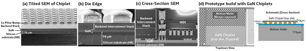
Technically, Intel says the chiplet was produced through a stealth dicing before grinding process that allowed the wafer to be thinned without damaging the already processed transistors and metal layers. The resulting structure kept transistor performance intact, according to Intel’s test data, with the company reporting gate lengths down to 30 nm, voltage blocking up to 78 V, and RF cut off frequencies above 300 GHz. Those figures point to a platform that is not only thin, but also relevant for high frequency and high efficiency switching applications.
Intel also says it built a full library of digital logic blocks directly on the GaN chiplet, including inverters, NAND gates, multiplexers, flip flops, and ring oscillators. The company reports that all of these circuits functioned correctly, with inverter switching speeds of 33 picoseconds, and says the results were consistent across the full 300 mm wafer. In practical terms, that means this is not just a materials demo. It is also a process integration story, showing that power devices and control logic can coexist on the same chiplet platform.
Reliability is another key part of the claim. Intel says the technology passed promising results in standard reliability evaluations including TDDB, pBTI, HTRB, and HCI testing, which are all important if a platform is ever going to move from research into real deployments. That does not mean products are imminent, but it does strengthen Intel’s argument that this is more than a laboratory curiosity.
From an industry angle, this announcement is especially relevant because GaN continues to attract attention as silicon approaches more of its physical and thermal limits in power conversion and high frequency operation. Intel argues that GaN can deliver higher power density, faster switching, and better high temperature stability than conventional silicon in these use cases, which could make it attractive for point of load power delivery close to processors, RF front ends for next generation wireless infrastructure, radar, satellite systems, and even photonic applications.
For the AI and server market, the value proposition is fairly easy to understand. Smaller, faster, and more efficient power delivery components placed closer to processors can reduce resistive losses and improve overall system efficiency, which becomes increasingly important as accelerators and dense compute platforms keep drawing more power. For telecom and networking, the promise is high frequency operation that better suits the centimeter wave and millimeter wave bands expected to matter more in future wireless systems. These are Intel’s proposed applications based on the demonstrated characteristics, not announced product launches.
This is still a research milestone, not a commercial product reveal, and that distinction matters. But it is the kind of milestone that signals where packaging, power delivery, and mixed material chiplet design are headed. If Intel can move this from demonstration to manufacturable deployment, the company could end up with a meaningful piece of future infrastructure in areas where efficiency, density, and thermal behavior matter as much as raw logic performance.
Do you think GaN chiplets will become one of the most important building blocks for future AI servers and 6G infrastructure, or will silicon still dominate longer than expected?