
Elon Musk Doubles Down on Tesla TeraFab Vision to Build Logic, Memory, and Packaging Under One Roof
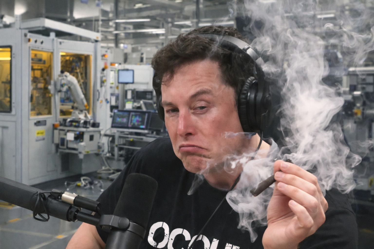
Tesla chief executive officer Elon Musk is once again putting a spotlight on the company’s ambition to control more of its semiconductor destiny, outlining a mega facility concept called TeraFab that would consolidate logic, memory, and packaging into a single domestic production footprint. The framing is simple and aggressive: Musk argues that rising supply constraints, combined with geopolitical tension across the global chip ecosystem, will force Tesla to pursue a more vertically integrated route if it wants to secure the volume of silicon it believes it will need over the next 3 to 4 years.
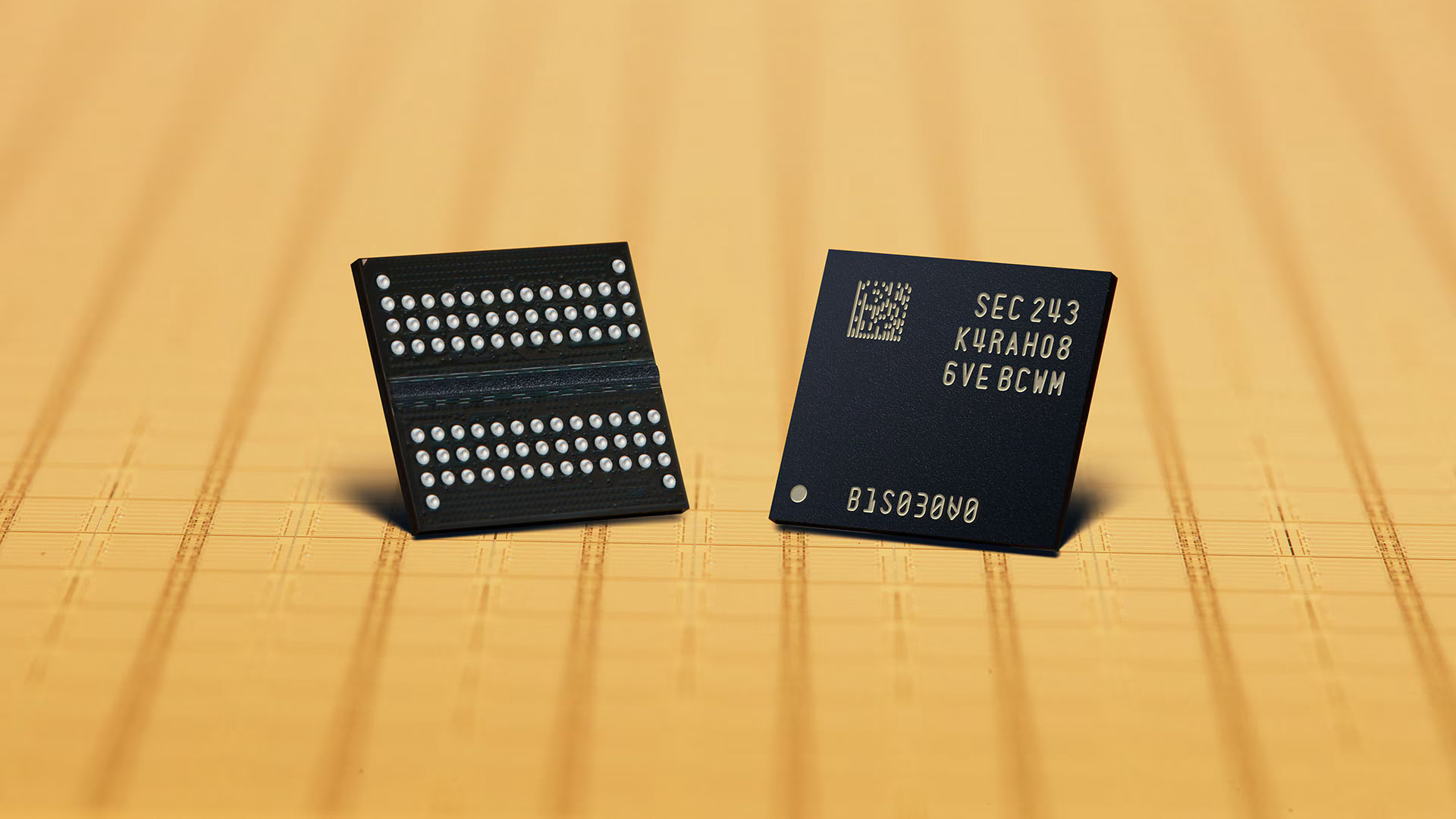
In Musk’s latest comments, he positioned TeraFab as a scale play designed to eliminate future bottlenecks, not just a vanity project. He described the goal as building a very large scale domestic chip facility that includes logic, memory, and packaging, insisting he does not see another way to hit the production volume Tesla is targeting. He has previously floated a vision of a fab network capable of outputting 100 billion to 200 billion chips per year, and the new language expands the scope beyond compute silicon alone into a full stack manufacturing model that would reduce reliance on external partners.
This proposal aligns with a broader trend across the industry: more companies are trying to de risk the supply chain by pulling critical capabilities closer to the core business, even if they do not fully internalize every layer. For Tesla, the strategic upside is clear. If the company can secure predictable access to compute at scale, it can more confidently execute long runway roadmaps tied to autonomy, physical AI, and dedicated training infrastructure.
At the same time, the execution risk is enormous. A modern semiconductor operation requires specialized talent, long lead time equipment procurement, and a capital plan that can handle both the initial build and the ongoing yield and process ramp realities. Musk acknowledged the difficulty directly, arguing that fabs are hard but that Tesla routinely takes on difficult projects, and that it would be crazy not to try.
There is also a second path that continues to surface as a more pragmatic compromise: partnering with an established foundry ecosystem while contributing capital to expand capacity and secure priority access. That approach could reduce the operational overhead of building an exclusive manufacturing network from scratch while still giving Tesla leverage and volume protection. It is the kind of hybrid strategy that could deliver many of the benefits of vertical integration without requiring Tesla to become a full service foundry operator overnight.
If Musk continues to push this narrative and ties it to Tesla’s next generation chip roadmap, TeraFab could become more than a headline. It could evolve into a strategic pillar that impacts how Tesla positions itself not only as an automotive and AI company, but as a semiconductor player with ambitions that reach beyond internal consumption.
Do you think Tesla should attempt a true end to end semiconductor facility with logic, memory, and packaging, or is a capital backed partnership with existing foundries the smarter play?