
Rambus Unveils PCIe 7.0 Switch IP With Time Division Multiplexing to Tackle AI Data Bottlenecks
Rambus is making a clear play for one of the most important pressure points in modern AI infrastructure: moving enough data fast enough to keep large compute clusters fully utilized. The company has introduced its new PCIe 7.0 Switch IP with Time Division Multiplexing, or TDM, and says the design is meant to address escalating bandwidth, latency, and scalability requirements across AI, cloud, and HPC systems. According to Rambus, the new switch is built to improve PCIe link utilization, reduce system complexity, and support the scale up and scale out demands of next generation distributed AI clusters.
The bigger issue Rambus is trying to solve is familiar to anyone following the AI server market. GPUs, accelerators, CPUs, and NVMe storage all need to exchange massive amounts of data continuously, and once infrastructure reaches large cluster scale, simply adding more bandwidth is no longer enough. Rambus says its PCIe 7.0 Switch IP with TDM helps system designers use available PCIe links more flexibly and efficiently while maintaining low latency and deterministic performance, especially in emerging disaggregated and pooled compute environments.
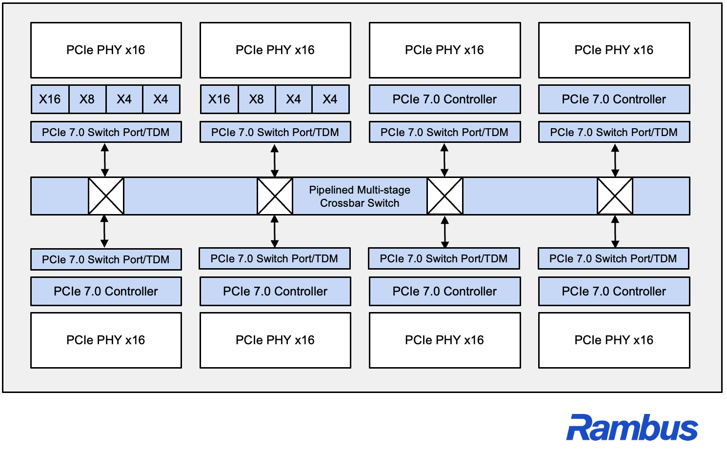
At the center of that pitch is TDM itself. Rambus says the switch can intelligently schedule and multiplex traffic across shared links, which is intended to maximize fabric utilization across different workload types, from large scale AI training to latency sensitive inference and heavy data movement. In plain terms, the company is arguing that PCIe fabrics need to become smarter about how traffic is allocated if designers want to avoid expensive accelerators sitting idle while waiting for data. That final interpretation is an inference based on Rambus’ technical description of link utilization and AI data movement challenges.
Rambus is also presenting this as more than a standalone block. The company says the new PCIe 7.0 Switch IP complements its broader PCIe 7.0 portfolio, which already includes controllers, retimers, and debug solutions. On its PCI Express product page, Rambus lists the PCIe 7.0 switch as a customizable multiport embedded switch for ASIC and FPGA implementations with TDM support, while its controller lineup reaches the PCIe 7.0 data rate of 128 GT/s and supports switch port, endpoint, and root port configurations.
That makes the announcement more relevant for custom silicon vendors and AI infrastructure builders than for end users directly. Rambus is selling IP, not finished add in cards or retail switches, so the real target here is the next generation of AI and data center SoCs that need more efficient internal and rack level connectivity. The company says the switch is designed for leading edge ASIC platforms and is aimed at customers trying to accelerate time to market while dealing with the growing performance, power, and reliability demands of modern AI systems.
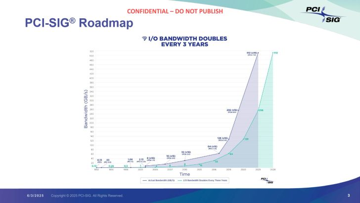
The timing also lines up with a broader industry trend. PCI Express bandwidth has kept increasing aggressively, with PCIe 7.0 doubling the lane rate again to 128 GT/s. Rambus’ own roadmap material continues to frame PCIe as a critical backbone for moving data between CPUs, GPUs, FPGAs, and specialized accelerators in AI and machine learning systems. What changes now is that simply having faster signaling is no longer the whole story. AI platforms are so large and traffic patterns are so uneven that smarter switching and scheduling are becoming just as important as raw line speed. That last point is an inference supported by Rambus’ description of AI bandwidth density, traffic management, and scalability demands.
Rambus also leaned on that message in its official statement, with Silicon IP chief Simon Blake Wilson saying that AI is reshaping system architectures and that it is no longer sufficient to just add more lanes or more endpoints. IDC’s Jeff Janukowicz echoed that position in the same announcement, saying that advanced PCIe switching technologies that improve link utilization and enable flexible traffic orchestration will be important as next generation interconnect technology evolves.
From a market perspective, this is a smart positioning move by Rambus. AI infrastructure conversations are often dominated by accelerators, memory, and networking silicon, but interconnect IP inside the system is becoming a much bigger differentiator as clusters scale and architectures become more disaggregated. If Rambus can convince ASIC and platform designers that TDM based PCIe switching meaningfully improves utilization and simplifies deployment, this kind of IP could become an important supporting layer in future AI servers and HPC fabrics. That is an inference based on the company’s stated target markets and the wider push toward larger, more modular AI infrastructure.
In short, Rambus is betting that the next wave of AI performance gains will not come only from faster chips, but from making sure those chips spend less time waiting on the fabric around them. PCIe 7.0 gives the raw speed boost, but TDM is Rambus’ attempt to make that bandwidth more usable in the real world, where the hardest problem is often not peak throughput on paper, but consistent data delivery under massive scale.
What do you think will matter more for future AI servers: faster interconnect standards, or smarter traffic management technologies like TDM layered on top of them?